
Analog and Digital Electronics 1st Module
MODULE 1: CLIPPERS AND CLAMPERS
Positive Series Clipper
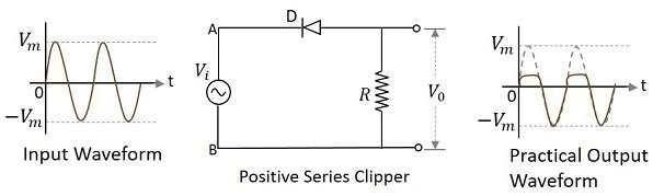
Clipper circuit in which the diode is connected in series to the input signal and that attenuates the positive portions of the waveform, is termed as Positive Series Clipper. The following figure represents the circuit diagram for positive series clipper.
Positive Cycle of the Input − When the input voltage is applied, the positive cycle of the input makes the point A in the circuit positive with respect to the point B. This makes the diode reverse biased and hence it behaves like an open switch. Thus the voltage across the load resistor becomes zero as no current flows through it and hence V0V0 will be zero.
Negative Cycle of the Input − The negative cycle of the input makes the point A in the circuit negative with respect to the point B. This makes the diode forward biased and hence it conducts like a closed switch. Thus the voltage across the load resistor will be equal to the applied input voltage as it completely appears at the output V0V0
Negative Series Clipper
A Clipper circuit in which the diode is connected in series to the input signal and that attenuates the negative portions of the waveform, is termed as Negative Series Clipper. The following figure represents the circuit diagram for negative series clipper.
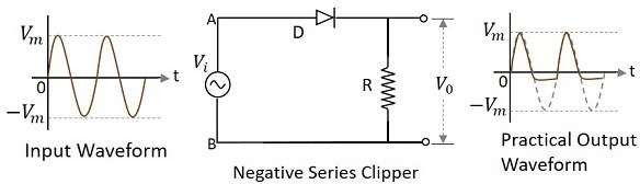
Positive Cycle of the Input − When the input voltage is applied, the positive cycle of the input makes the point A in the circuit positive with respect to the point B.
This makes the diode forward biased and hence it acts like a closed switch. Thus the input voltage completely appears across the load resistor to produce the output V0.
Negative Cycle of the Input − The negative cycle of the input makes the point A in the circuit negative with respect to the point B. This makes the diode reverse biased and hence it acts like an open switch. Thus, the voltage across the load resistor will be zero making V0 zero.
Two-way Clipper or Double Ended Shunt clipper
This is a positive and negative clipper with a reference voltage Vr. The input voltage is clipped two-way both positive and negative portions of the input waveform with two reference voltages. For this, two diodes D1 and D2 along with two reference voltagesVr1 and Vr2 are connected in the circuit.
This circuit is also called as a Combinational Clipper circuit. The figure below shows the circuit arrangement for a two-way or a combinational clipper circuit along with its output waveform.
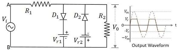
During the positive half of the input signal, the diode D1 conducts making the reference voltage Vr1 appear at the output.
During the negative half of the input signal, the diode D2 conducts making the reference voltage Vr1 appear at the output.
Hence both the diodes conduct alternatively to clip the output during both the cycles. The output is taken across the load resistor.
Positive Clamper Circuit
A Clamping circuit restores the DC level. When a negative peak of the signal is raised above to the zero level, then the signal is said to be positively clamped.
A Positive Clamper circuit is one that consists of a diode, a resistor and a capacitor and that shifts the output signal to the positive portion of the input signal. The figure below explains the construction of a positive clamper circuit.
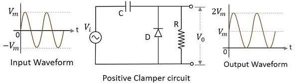
Initially when the input is given, the capacitor is not yet charged and the diode is reverse biased. The output is not considered at this point of time. During the negative half cycle, at the peak value, the capacitor gets charged with negative on one plate and positive on the other. The capacitor is now charged to its peak value Vm. The diode is forward biased and conducts heavily.
During the next positive half cycle, the capacitor is charged to positive Vm while the diode gets reverse biased and gets open circuited. The output of the circuit at this moment will be
V0=Vi+VmV0=Vi+Vm
Hence the signal is positively clamped as shown in the above figure. The output signal changes according to the changes in the input, but shifts the level according to the charge on the capacitor, as it adds the input voltage.
Negative Clamper
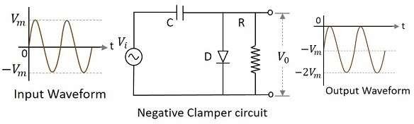
A Negative Clamper circuit is one that consists of a diode, a resistor and a capacitor and that shifts the output signal to the negative portion of the input signal. The figure below explains the construction of a negative clamper circuit.
During the positive half cycle, the capacitor gets charged to its peak value vm. The diode is forward biased and conducts. During the negative half cycle, the diode gets reverse biased and gets open circuited. The output of the circuit at this moment will be
V0=Vi+VmV0=Vi+Vm
Hence the signal is negatively clamped as shown in the above figure. The output signal changes according to the changes in the input, but shifts the level according to the charge on the capacitor, as it adds the input voltage.
Applications
There are many applications for both Clippers and Clampers such as
Clippers
· Used for the generation and shaping of waveforms
· Used for the protection of circuits from spikes
· Used for amplitude restorers
· Used as voltage limiters
· Used in television circuits
· Used in FM transmitters
Clampers
· Used as direct current restorers
· Used to remove distortions
· Used as voltage multipliers
· Used for the protection of amplifiers
· Used as test equipment
· Used as base-line stabilizer
RC Coupled BJT Amplifier
The constructional details of a two-stage RC coupled transistor amplifier circuit are as follows. The two stage amplifier circuit has two transistors, connected in CE configuration and a common power supply VCC is used. The potential divider network R1 and R2and the resistor Reform the biasing and stabilization network. The emitter by-pass capacitor Ce offers a low reactance path to the signal.
The resistor RL is used as a load impedance. The input capacitor C in present at the initial stage of the amplifier couples AC signal to the base of the transistor. The capacitor CC is the coupling capacitor that connects two stages and prevents DC interference between the stages and controls the shift of operating point. The figure below shows the circuit diagram of RC coupled amplifier.
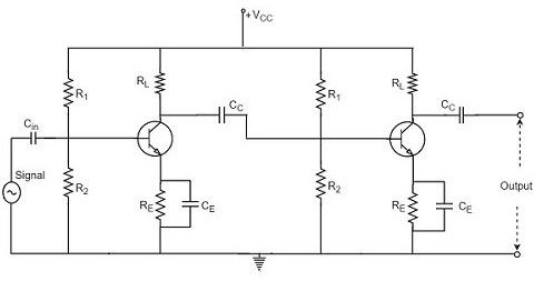
Operation of RC Coupled Amplifier
When an AC input signal is applied to the base of first transistor, it gets amplified and appears at the collector load RL which is then passed through the coupling capacitor CC to the next stage. This becomes the input of the next stage, whose amplified output again appears across its collector load. Thus the signal is amplified in stage by stage action.
The important point that has to be noted here is that the total gain is less than the product of the gains of individual stages. This is because when a second stage is made to follow the first stage, the effective load resistance of the first stage is reduced due to the shunting effect of the input resistance of the second stage. Hence, in a multistage amplifier, only the gain of the last stage remains unchanged.
As we consider a two stage amplifier here, the output phase is same as input. Because the phase reversal is done two times by the two stage CE configured amplifier circuit.
Frequency Response of RC Coupled Amplifier
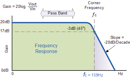
Frequency response curve is a graph that indicates the relationship between voltage gain and function of frequency. The frequency response of a RC coupled amplifier is as shown in the following graph.
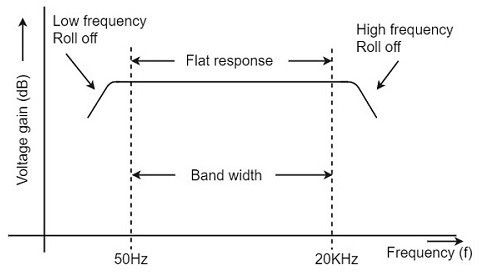
From the above graph, it is understood that the frequency rolls off or decreases for the frequencies below 50Hz and for the frequencies above 20 KHz. whereas the voltage gain for the range of frequencies between50Hz and 20 KHz is constant.
We know that,
XC=12πfc X C=12πfc
It means that the capacitive reactance is inversely proportional to the frequency.
At Low frequencies (i.e. below 50 Hz)
The capacitive reactance is inversely proportional to the frequency. At low frequencies, the reactance is quite high.
At High frequencies (i.e. above 20 KHz)
Again considering the same point, we know that the capacitive reactance is low at high frequencies. So, a capacitor behaves as a short circuit, at high frequencies
At Mid-frequencies (i.e. 50 Hz to 20 KHz)
The voltage gain of the capacitors is maintained constant in this range of frequencies, as shown in figure. If the frequency increases, the reactance of the capacitor CC decreases which tends to increase the gain. But this lower capacitance reactive increases the loading effect of the next stage by which there is a reduction in gain.
Due to these two factors, the gain is maintained constant
Advantages of RC Coupled Amplifier
The following are the advantages of RC coupled amplifier.
· The frequency response of RC amplifier provides constant gain over a wide frequency range, hence most suitable for audio applications.
· The circuit is simple and has lower cost because it employs resistors and capacitors which are cheap.
· It becomes more compact with the upgrading technology.
Disadvantages of RC Coupled Amplifier
The following are the disadvantages of RC coupled amplifier.
· The voltage and power gain are low because of the effective load resistance.
· They become noisy with age.
· Due to poor impedance matching, power transfer will be low.
Applications of RC Coupled Amplifier
The following are the applications of RC coupled amplifier.
· They have excellent audio fidelity over a wide range of frequency.
· Widely used as Voltage amplifiers
· Due to poor impedance matching, RC coupling is rarely used in the final stages.
Op-Amp active filters
I order low pass filter: Design, frequency scaling,
Active Low Pass Filter
The most common and easily understood active filter is the Active Low Pass Filter. Its principle of operation and frequency response is exactly the same as those for the previously seen passive filter, the only difference this time is that it uses an op-amp for amplification and gain control. The simplest form of a low pass active filter is to connect an inverting or non-inverting amplifier, the same as those discussed in the Op-amp tutorial, to the basic RC low pass filter circuit as shown.
First Order Low Pass Filter
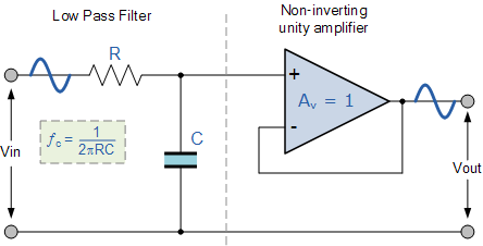
This first-order low pass active filter, consists simply of a passive RC filter stage providing a low frequency path to the input of a non-inverting operational amplifier. The amplifier is configured as a voltage-follower (Buffer) giving it a DC gain of one, Av = +1 or unity gain as opposed to the previous passive RC filter which has a DC gain of less than unity.
The advantage of this configuration is that the op-amps high input impedance prevents excessive loading on the filters output while its low output impedance prevents the filters cut-off frequency point from being affected by changes in the impedance of the load.
While this configuration provides good stability to the filter, its main disadvantage is that it has no voltage gain above one. However, although the voltage gain is unity the power gain is very high as its output impedance is much lower than its input impedance. If a voltage gain greater than one is required we can use the following filter circuit.
Frequency Response Curve
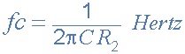
If the external impedance connected to the input of the filter circuit changes, this impedance change would also affect the corner frequency of the filter (components connected together in series or parallel). One way of avoiding any external influence is to place the capacitor in parallel with the feedback resistor R2 effectively removing it from the input but still maintaining the filters characteristics.
However, the value of the capacitor will change slightly from being 100nF to 110nF to take account of the 9k1Ω resistor, but the formula used to calculate the cut-off corner frequency is the same as that used for the RC passive low pass filter.
II order low pass filter:
As with the passive filter, a first-order low-pass active filter can be converted into a second-order low pass filter simply by using an additional RC network in the input path. The frequency response of the second-order low pass filter is identical to that of the first-order type except that the stop band roll-off will be twice the first-order filters at 40dB/decade (12dB/octave). Therefore, the design steps required of the second-order active low pass filter are the same.
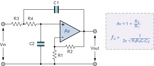
Second-order Active Low Pass Filter Circuit
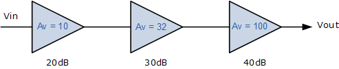
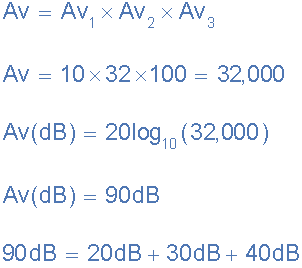
When cascading together filter circuits to form higher-order filters, the overall gain of the filter is equal to the product of each stage. For example, the gain of one stage may be 10 and the gain of the second stage may be 32 and the gain of a third stage may be 100. Then the overall gain will be 32,000, (10 x 32 x 100) as shown below.
Cascading Voltage Gain
Second-order (two-pole) active filters are important because higher-order filters can be designed using them. By cascading together first and second-order filters, filters with an order value, either odd or even up to any value can be constructed.
First Order High Pass Filter
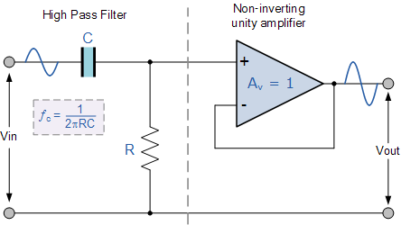
Technically, there is no such thing as an active high pass filter. Unlike Passive High Pass Filters which have an “infinite” frequency response, the maximum pass band frequency response of an active high pass filter is limited by the open-loop characteristics or bandwidth of the operational amplifier being used, making them appear as if they are band pass filters with a high frequency cut-off determined by the selection of op-amp and gain.
In the Operational Amplifier tutorial we saw that the maximum frequency response of an op-amp is limited to the Gain/Bandwidth product or open loop voltage gain ( A V ) of the operational amplifier being used giving it a bandwidth limitation, where the closed loop response of the op amp intersects the open loop response.
A commonly available operational amplifier such as the uA741 has a typical “open-loop” (without any feedback) DC voltage gain of about 100dB maximum reducing at a roll off rate of -20dB/Decade (-6db/Octave) as the input frequency increases. The gain of the uA741 reduces until it reaches unity gain, (0dB) or its “transition frequency” ( ƒt ) which is about 1MHz. This causes the op-amp to have a frequency response curve very similar to that of a first-order low pass filter and this is shown below.
Frequency response curve of a typical Operational Amplifier
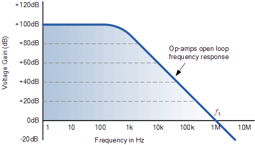
Then the performance of a “high pass filter” at high frequencies is limited by this unity gain crossover frequency which determines the overall bandwidth of the open-loop amplifier. The gain-bandwidth product of the op-amp starts from around 100kHz for small signal amplifiers up to about 1GHz for high-speed digital video amplifiers and op-amp based active filters can achieve very good accuracy and performance provided that low tolerance resistors and capacitors are used.
Under normal circumstances the maximum pass band required for a closed loop active high pass or band pass filter is well below that of the maximum open-loop transition frequency. However, when designing active filter circuits it is important to choose the correct op-amp for the circuit as the loss of high frequency signals may result in signal distortion.
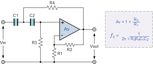
Second-order Active High Pass Filter Circuit
Higher-order high pass active filters, such as third, fourth, fifth, etc are formed simply by cascading together first and second-order filters. For example, a third order high pass filter is formed by cascading in series first and second order filters, a fourth-order high pass filter by cascading two second-order filters together and so on.
Then an Active High Pass Filter with an even order number will consist of only second-order filters, while an odd order number will start with a first-order filter at the beginning as shown.
Cascading Active High Pass Filters
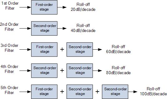
Although there is no limit to the order of a filter that can be formed, as the order of the filter increases so to does its size. Also, its accuracy declines, that is the difference between the actual stop band response and the theoretical stop band response also increases.
If the frequency determining resistors are all equal, R1 = R2 = R3 etc, and the frequency determining capacitors are all equal, C1 = C2 = C3 etc, then the cut-off frequency for any order of filter will be exactly the same. However, the overall gain of the higher-order filter is fixed because all the frequency determining components are equal.
Wide Band pass filter,
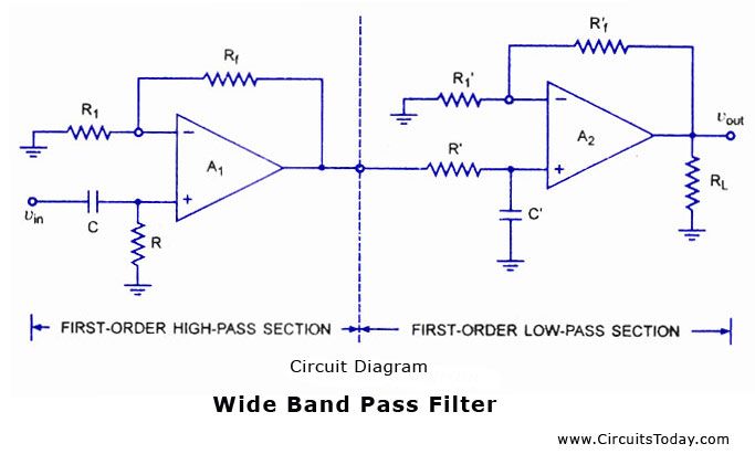
A wide bandpass filter can be formed by simply cascading high-pass and low-pass sections and is generally the choice for simplicity of design and performance though such a circuit can be realized by a number of possible circuits. To form a ± 20 db/ decade bandpass filter, a first-order high-pass and a first-order low-pass sections are cascaded; for a ± 40 db/decade bandpass filter, second-order high- pass filter and a second-order low-pass filter are connected in series, and so on. It means that, the order of the bandpass filter is governed by the order of the high-pass and low-pass filters it consists of.
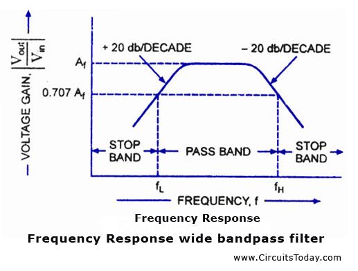
A ± 20 db/decade wide bandpass filter composed of a first-order high-pass filter and a first-order low-pass filter, is illustrated in fig. (a). Its frequency response is illustrated in fig. (b)..
Narrow band pass filter,
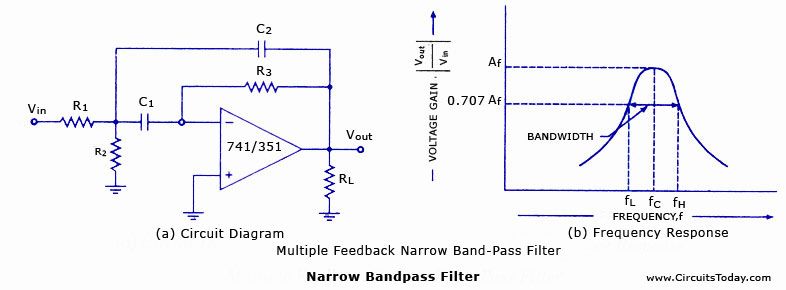
A narrow bandpass filter employing multiple feedback is depicted in figure. This filter employs only one op-amp, as shown in the figure. In comparison to all the filters discussed so far, this filter has some unique features that are given below.
1. It has two feedback paths, and this is the reason that it is called a multiple-feedback filter.
2. The op-amp is used in the inverting mode.
The frequency response of a narrow bandpass filter is shown in fig(b)
Generally, the narrow bandpass filter is designed for specific values of centre frequency fc and Q or fc and BW. The circuit components are determined from the following relationships. For simplification of design calculations each of C1 and C2 may be taken equal to C.
Band reject filter:
The bandpass filter passes one set of frequencies while rejecting all others. The band-stop filter does just the opposite. It rejects a band of frequencies, while passing all others. This is also called a band-reject or band-elimination filter. Like bandpass filters, band-stop filtersmay also be classified as (i) wide-band and (ii) narrow band reject filters.
Wide Band reject filter,
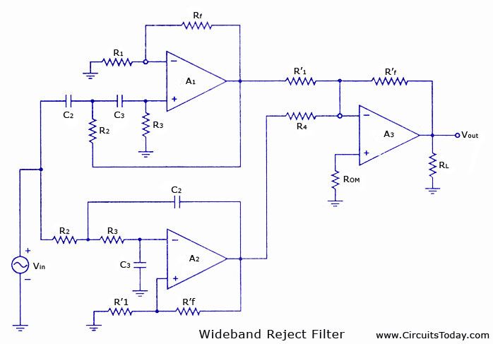
A wide band-stop filter using a low-pass filter, a high-pass filter and a summing amplifier is shown in figure. For a proper band reject response, the low cut-off frequency fL of high-pass filter must be larger than the high cut-off frequency fH of the low-pass filter. In addition, the passband gain of both the high-pass and low-pass sections must be equal.
Narrow band reject filter,
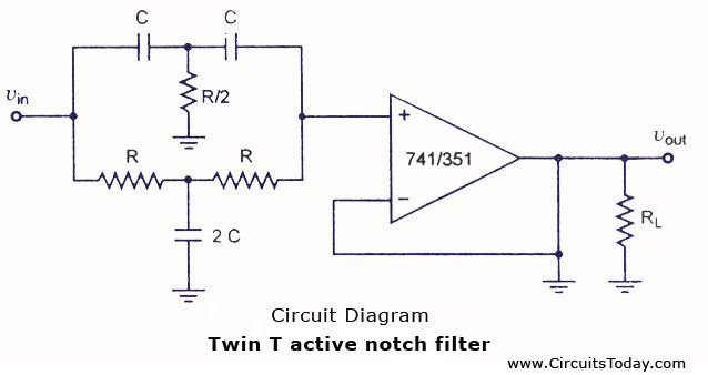
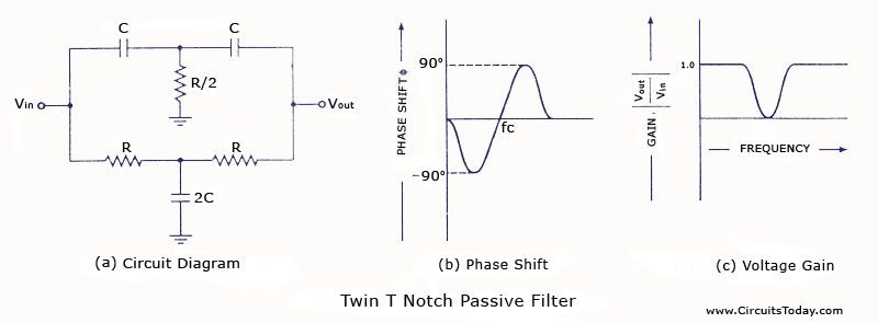
This is also called a notch filter. It is commonly used for attenuation of a single frequency such as 60 Hz power line frequency hum. The most widely used notch filter is the twin-T network illustrated in fig. (a). This is a passive filter composed of two T-shaped networks. One T-network is made up of two resistors and a capacitor, while the other is made of two capacitors and a resistor. One drawback of above notch filter (passive twin-T network) is that it has relatively low figure of merit Q. However, Q of the network can be increased significantly if it is used with the voltage follower, as illustrated in fig. (a). Here the output of the voltage follower is supplied back to the junction of R/2 and 2 C. The frequency response of the active notch filter is shown in fig (b).
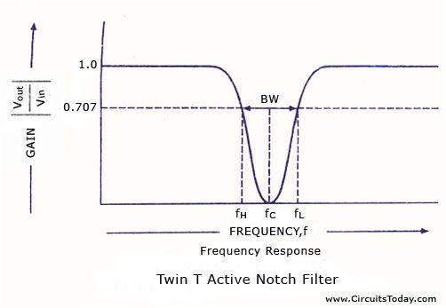
Notch filters are most commonly used in communications and biomedical instruments for eliminating the undesired frequencies.

