
Analog and Digital Electronics 3rd Module
MODULE 3 – 555 timers and its applications 555 Timer
The 555 Timer IC got its name from the three 5KΩ resistors that are used in its voltage divider network. This IC is useful for generating accurate time delays and oscillations. This chapter explains about 555 Timer in detail.
555 timer pin diagram and architecture of 555 timers
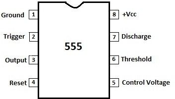
Pin 1: Grounded Terminal: All the voltages are measured with respect to the Ground terminal.
Pin 2: Trigger Terminal: The trigger pin is used to feed the trigger input hen the 555 IC is set up as a monostable multivibrator. This pin is an inverting input of a comparator and is responsible for the transition of flip-flop from set to reset. The output of the timer depends on the amplitude of the external trigger pulse applied to this pin. A negative pulse with a dc level greater than Vcc/3 is applied to this terminal. In the negative edge, as the trigger passes through Vcc/3, the output of the lower comparator becomes high and the complimentary of Q becomes zero. Thus the 555 IC output gets a high voltage, and thus a quasi stable state.
Pin 3: Output Terminal: Output of the timer is available at this pin. There are two ways in which a load can be connected to the output terminal. One way is to connect between output pin (pin 3) and ground pin (pin 1) or between pin 3 and supply pin (pin 8). The load connected between output and ground supply pin is called the normally on load and that connected between output and ground pin is called the normally off load.
Pin 4: Reset Terminal: Whenever the timer IC is to be reset or disabled, a negative pulse is applied to pin 4, and thus is named as reset terminal. The output is reset irrespective of the input condition. When this pin is not to be used for reset purpose, it should be connected to
+ VCC to avoid any possibility of false triggering.
Pin 5: Control Voltage Terminal: The threshold and trigger levels are controlled using this pin. The pulse width of the output waveform is determined by connecting a POT or bringing in an external voltage to this pin. The external voltage applied to this pin can also be used to modulate the output waveform. Thus, the amount of voltage applied in this terminal will decide when the comparator is to be switched, and thus changes the pulse width of the output. When this pin is not used, it should be bypassed to ground through a 0.01 micro Farad to avoid any noise problem.
Pin 6: Threshold Terminal: This is the non-inverting input terminal of comparator 1, which compares the voltage applied to the terminal with a reference voltage of 2/3 VCC. The amplitude of voltage applied to this terminal is responsible for the set state of flip-flop.
When the voltage applied in this terminalis greater than 2/3Vcc, the upper comparator switches to +Vsat and the output gets reset.
Pin 7 : Discharge Terminal: This pin is connected internally to the collector of transistor and mostly a capacitor is connected between this terminaland ground. It is called discharge terminalbecause when transistorsaturates, capacitor dischargesthrough the transistor.
When the transistor is cut-off, the capacitor charges at a rate determined by the external resistor and capacitor.
Pin 8: Supply Terminal: A supply voltage of + 5 V to + 18 V is applied to this terminal with respect to ground (pin 1).
555 timer as monostable multivibrator
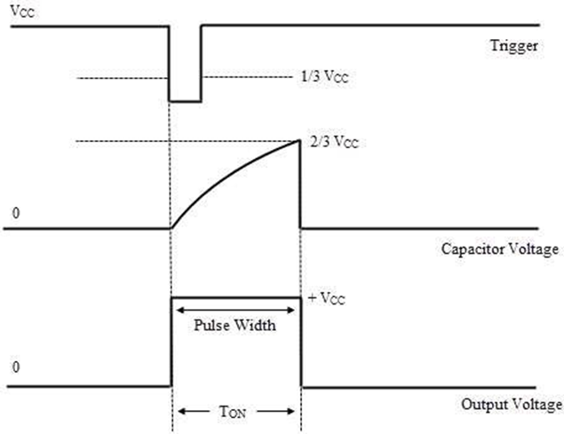
The monostable mode is also called “one-shot” pulse generator. The sequence of events starts when a negative going trigger pulse is applied to the trigger comparator. When this trigger comparator senses the short negative going trigger pulse to be just below the reference voltage (1/3 VCC), the device triggers and the output goes HIGH.
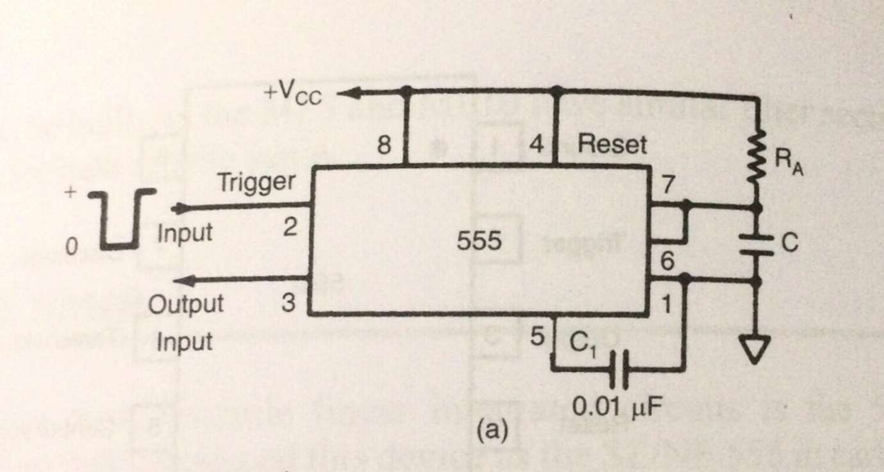
The discharge transistor is turned OFF and the capacitor C that is externally connected to its collector will start charging to the max value through the resistor R. The HIGH output pulse ends when the charge on the capacitor reaches 2/3 VCC. The internal connection of the IC 555 in monostable mode along with the RC timing circuit is shown below.
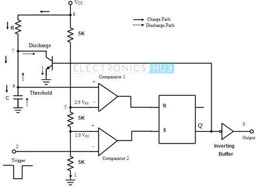
The detailed operation can be explained as follows. Initially, the flip-flop is RESET. This will allow the discharge transistor to go to saturation. The capacitor C, which is connected to the open collector (drain in case of CMOS) of the transistor, is provided with a discharge path.
Hence the capacitor discharges completely and the voltage across it is 0. The output at pin 3 is low (0).
When a negative going trigger pulse input is applied to the trigger comparator (comparator 2), it is compared with a reference voltage of 1/3 VCC. The output remains low until the trigger input is greater than the reference voltage. The moment trigger voltage goes below 1/3 VCC, the output of comparator goes high and this will SET the flip-flop. Hence the output at pin 3 will become high.
At the same time, the discharge transistor is turned OFF and the capacitor C will begin to charge and the voltage across it rises exponentially. This is nothing but the threshold voltage at pin 6. This is given to the comparator 1 along with a reference voltage of 2/3 VCC. The output at pin 3 will remain HIGH until the voltage across the capacitor reaches2/3 VCC.
The instanceat which the threshold voltage (which is nothing but the voltage across the capacitor) becomes more than the reference voltage, the output of the comparator 1 goes high. This will RESET the flip-flop and hence the output at pin 3 will fall to low (logic 0) i.e. the output returns to its stable state. As the output is low, the discharge transistor is driven to saturation and the capacitor will completely discharge.
Thus the output returns back to stable state from quasi-stable state.
The output of the Monostable Multivibrator remains low until a trigger pulse is again applied. Then the cycle repeats. Trigger input, output voltage and capacitor voltage waveforms are shown in figure.
Pulse Width Derivation
We know that the voltage across the capacitor C rises exponentially. Hence the equation for the capacitor voltage VC can be written as
VC = VCC (1 – e-t/RC)
When the capacitor voltage is 2/3 VCC, then 2/3 VCC = VCC (1 – e-t/RC)
2/3 = 1 – e-t/RC e-t/RC = 1/3
– t/RC = ln (1/3)
– t/RC = -1.098 t = 1.098 RC
∴ t ≈ 1.1 RC
The pulse width of the output rectangular pulse is W = 1.1 RC. The waveforms of the monostable operation are shown below.
Monostable Multivibrator Applications
a) Frequency divider
The monostable multivibrator of figure can be used as a frequency divider by adjusting the length of the timing cycle tp with respect to the time period T of the trigger input signal applied top in 2.
To use the monostable multivibrator as a divide-by-2 circuit, the timing interval tp must be slighlty larger than the time period T of the trigger input signal, By the same concept, to use the monostable multivibrator as a divide-by-3 circuit, tp must be slightly larger than twice the period of the input trigger signal, and so on
The frequency-divider application is possible because the monostable multivibrator cannot be triggered during the timing cycle.
b) Pulse stretcher
This application makes use of the fact that the output pulse width (timing interval) of the monostable multivibrator is of longer duration than the negative pulse width of the input trigger. As such, the output pulse width of the monostable multivibrator can be viewed as a stretched version of the narrow input pulse, hence the name pulse stretcher.
Often, narrow-pulse-width signals are not suitable for driving an LED display, mainly because of their very narrow pulse widths. In other words, the LED may be flashing but not visible to the eye because its on time is infinitesimally small compared to its off time. The 555 pulse stretcher can be used to remedy this problem.
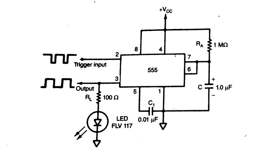
Fig shows a basic monostable used as a pulse generator with an LED indicator at output
The 555 as an Astable Multivibrator
An astable multivibrator, often called a free-running multivibrator, is a rectangular wave generating circuit. Unlike the monostable multivibrator, this circuit does not require an external trigger to change the state of output, hence the name free running.
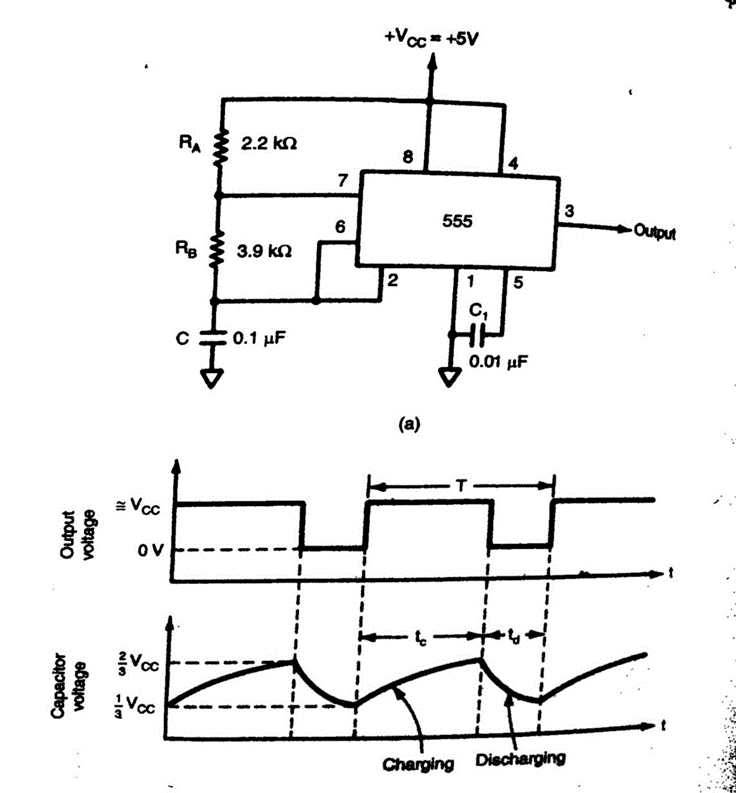
Fig 9-21 a shows the 555 timer connected as an astable multivibrator. Initially, when the output is high, capacitor C starts charging towards VCC through RA and RB. However as soon as voltage across the capacitor equals 2/3 VCC, Now comparator C starts discharging through RB and transistor Q1,
When the voltage across C equals 1/3 VCC, comparator 2’s output triggers the flip-flop, and the output goes high. Then the cycle repeats. The output voltage and capacitor voltage waveforms are shown in fig 9-21(b)
As shown in fig, the capacitor is periodically charged and discharged between 2/3 VCC and 1/3 VCC respectively. The time during which the capacitor charges from 1/3 VCC to 2/3 VCC is equal to the time the output is high and is given by
tc = 0.69(RA + RB)C ….. (1)
where RA and RB are in ohms and C is in farads. Similarly, the time during which the capacitor discharges from 2/3 VCC to 1/3 VCC is equal to the time the output is low and is given by
ttd = 0.69(RB)C ……(2)
where RB is in ohms and C is in farads. Thus the total period of the output waveform is
T= tc +td = 0.69(RA + 2RB)C …(3)
This in turn, gives the frequency of oscillation as

Equation 4 indicates that the frequency is fo is independent of the supply voltage VCC.
Often the term duty cycle is used in conjuction with the astable multivibrator. The duty cycle is the ratio of the time tc during which the output is high to the toal time period T.
It is generally expresed as percentage. In equation form

Astable Multivibrator Applications
a) Square wave oscillator
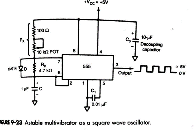
Without reducing RA = 0𝛺, the astable multivibrator can be used to produce a square wave output simply by connecting diode D across resistor RB, as shown in fig. The capacitor C charges through RA and diode D to approximately 2/3 VCC and discharges through RB and terminal 7 (transistor Q1) until the capacitor voltage equals approximately 1/3 VCC then the cycle repeats.
To obtain a square wave output(50%duty cycle ), RA must be a combination of a fixed resistor and potentiometer so that the potentiometer can be adjusted for the exact square wave.
b) Free running ramp generator
The astable multivibrator can be used as a free running ramp generator when resistors RA and RB are replaced by a current mirror. Fig 9.24 a shows an astable multivibrator configured to perform this function.
The current mirror starts charging capacitor toward VCC at a constant rate. When voltage across C equals 2/3 VCC, comparator1 turns transistor Q1 on,and C rapidly discharges through transistor Q1 on and C rapidly discharges through transistor Q1.
However, when the discharge voltage across C is approximately equal to 1/3 VCC, comparator 2 switches transistor Q1 off, and then capacitor C stars charging up again. Thus the charge-discharge cycle keeps repeating. The discharging time of the capacitor is relatively negligible compared to its charging time

Applications of 555 timer
1) Frequency divider
2) Pulse Stretcher
3) Square Wave oscillator
4) Free running ramp generator
5) Timer Switch

