Analog and Digital Electronics 4th Module
Combinational Logic: Introduction to K-Maps: 2,3 and 4 variable maps, (Youtube and teachers will help you in this)
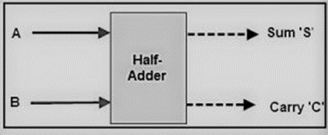
Adders: Half adder and Full adder,
An adder is a digital logic circuit in electronics that is extensively used for the addition of numbers. In many computers and other types of processors, adders are even used to calculate addresses and related activities and calculate table indices in the ALU and even utilized in other parts of the processors. These can be built for many numerical representations like excess-3 or binary coded decimal. Adders are basically classified into two types: Half Adder and Full Adder
Half Adder
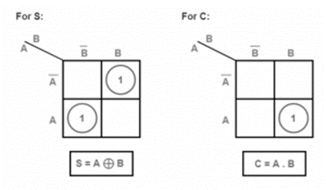
The half adder circuit has two inputs: A and B, which add two input digits and generates a carry and a sum.
So, coming to the scenario of half adder, it adds two binary digits where the input bits are termed as augend and addend and the result will be two outputs one is the sum and the other is carry. To perform the sum operation, XOR is applied to both the inputs, and AND gate is applied to both inputs to produce carry.
The 2-bit half adder truth table is as below:

The carry output is 0 unless both inputs are 1. The S output represents the least significant bit of the sum.
The simplified Boolean functions for the two outputs can be obtained directly from the truth table. The simplified sum of products expressions are
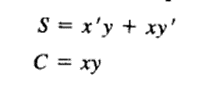
Various implementation of half adder is shown in figures below

Fig 4-2 (a) as mentioned before, is the implementation of half adder in sum of products.
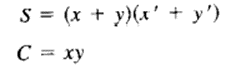
Fig 4-2(b) shows the implementation in product of sums:
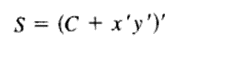
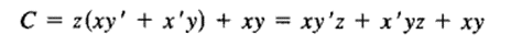
To obtain the implementation of Fig 4-2(c) we note that S is the exclusive OR of x and y. The complement of S is the equivalence of x and y.
But C =xy and therefore, we have
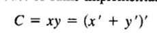
In fig 4-2(d) we use the product of sums implementation with C derived as follows:
The half adder can be implemented with an exclusive OR and an AND gate as shown in fig (e)
Full Adder
This adder is difficult to implement when compared to half-adder.

The difference between a half-adder and a full-adder is that the full-adder has three inputs and two outputs, whereas half adder has only two inputs and two outputs. The first two inputs are A and B and the third input is an input carry as C-IN. When a full-adder logic is designed, you string eight of them together to create a byte-wide adder and cascade the carry bit from one adder to the next.
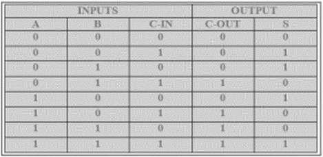
The output carry is designated as C-OUT and the normal output is represented as S which is ‘SUM’.
With the above full adder truth-table, the implementation of a full adder circuit can be understood easily.
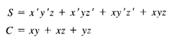
Fig shows the implementation of a full adder in sum of products

This implementation uses the following Boolean expressions:

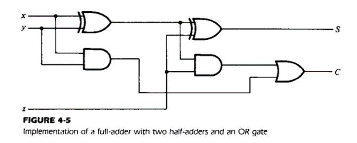
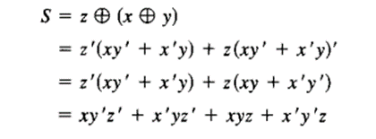
This implementation shows full adder with two half adders and an OR gate
This implementation uses the following Boolean expressions:
And the carry output is
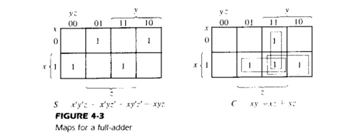
Half Adder and Full Adder using K-Map
Even the sum and carry outputs for half adder can also be obtained with the method of Karnaugh map (K-map). The half adder and full adder boolean expression can be obtained through K-map. So, the K-map for these adders is discussed below.
The half adder K-map is
The full adder K-Map is
Difference between Half Adder and Full Adder
The difference between the half adder and full adder table is shown below.

Subtractor:
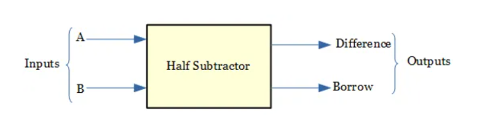
Half subtractor
The half-subtractor subtracts two bits and produces an output as difference and borrow. It needs two binary inputs(subtrahend bit and minuend bit), two binary outputs(difference and borrow) and combination of logic circuit.
It performs subtraction operation of two bits. Four possible operations are possible with the two inputs and produces four outputs, as shown below.
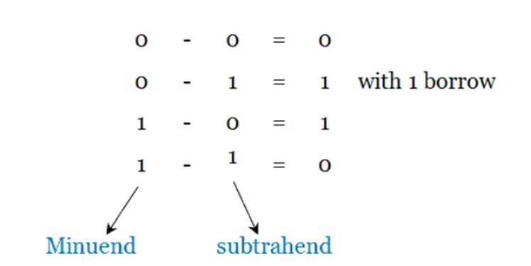
As you can see above, if the minuend bit is higher than the subtrahend bit, difference output is produced with no borrow. If the subtrahend bit is higher than the minuend bit, difference output is produced with borrow.
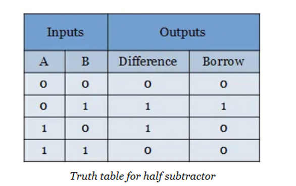
The boolean expression for the outputs of half-subtractor can be determined by constructing a truth table. The truth table for half adder is shown below.
For difference and borrow outputs, a boolean expression has to be derived using Karnaugh map. Since it has only two input variables, 4-cells k-map is used to simplify. Learn how to Minimize a Boolean function using k-map.
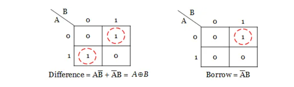
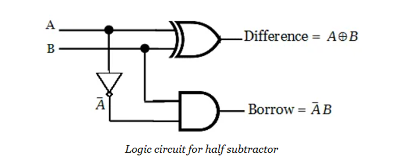
The obtained boolean expression for difference output is an Ex-OR gate output. The Logic circuit diagram for a half subtractor circuit is draw from the boolean expression.
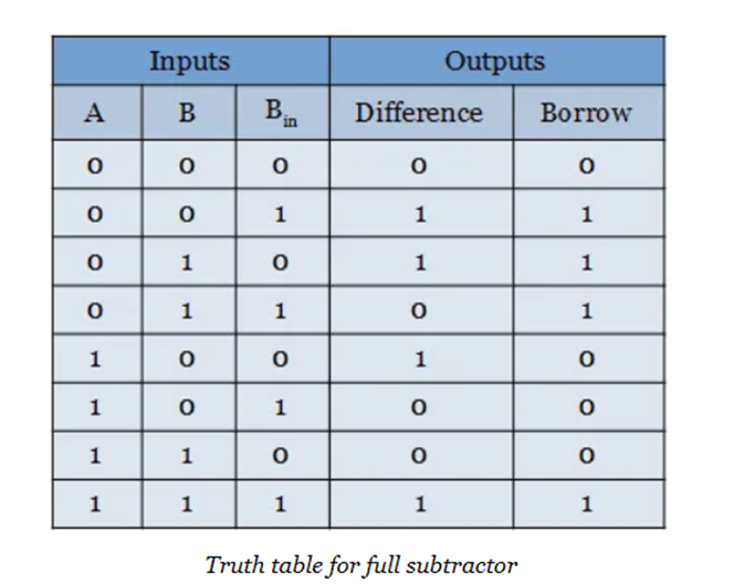
Full subtractor
Full subtractor
A full subtractor has three binary inputs(subtrahend, minuend and one borrow bit from the previous subtraction operation). It produces two binary outputs(difference and borrow) using a combination of logic gates. The borrow given to the previous subtraction operation is denoted as Bin

In full subtractor, eight possible operations are possible with three inputs and produces eight, two digit outputs. The operation is shown in the truth table below.
For difference and borrow outputs, boolean expression has to be derived using Karnaugh map. Since it has three input variables, 8-cells k-map is used to simplify the expression.
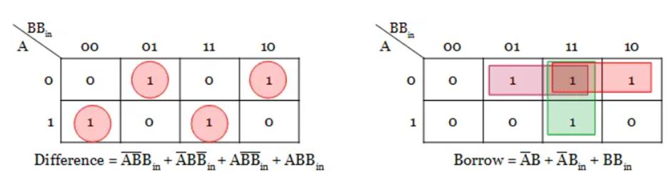
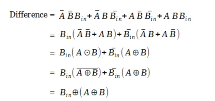
The Boolean expression for difference output can further be simplified as follows.
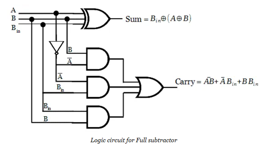
Now we have two boolean expressions for difference and borrow output. With those expressions, the combinational circuit for full subtractor is implemented.
Realization of full subtractor using two half subtractor

Multiplexers:
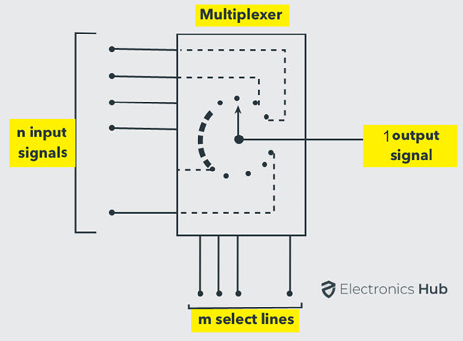
The multiplexer or MUX is a digital switch, also called as data selector. It is a Combinational Logic Circuit with more than one input line, one output line and more than one select line. It accepts the binary information from several input lines or sources and depending on the set of select lines, a particular input line is routed onto a single output line.
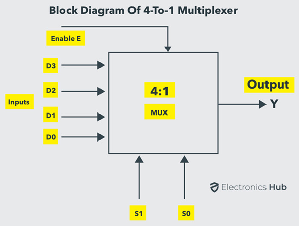
4-to-1 Multiplexer
A 4-to-1 multiplexer consists four data input lines as D0 to D3, two select lines as S0 and S1 and a single output line Y. The select lines S0 and S1 select one of the four input lines to connect the output line. The figure below shows the block diagram of a 4-to-1 multiplexer in which, the multiplexer decodes the input through select line.
The truth table of a 4-to-1 multiplexer is shown below in which four input combinations 00, 10, 01 and 11 on the select lines respectively switches the inputs D0, D2, D1 and D3 to the output. That means when S0=0 and S1 =0, the output at Y is D0, similarly Y is D1 if the select inputs S0=0 and S1= 1 and so on.
|
S0 |
S1 |
D0 |
D1 |
D2 |
D3 |
Y |
|
0 |
0 |
0 |
X |
X |
X |
0 |
|
0 |
0 |
1 |
X |
X |
X |
1 |
|
0 |
1 |
X |
0 |
X |
X |
0 |
|
0 |
1 |
X |
1 |
X |
X |
1 |
|
1 |
0 |
X |
X |
0 |
X |
0 |
|
1 |
0 |
X |
X |
1 |
X |
1 |
|
1 |
1 |
X |
X |
X |
0 |
0 |
|
1 |
1 |
X |
X |
X |
1 |
1 |
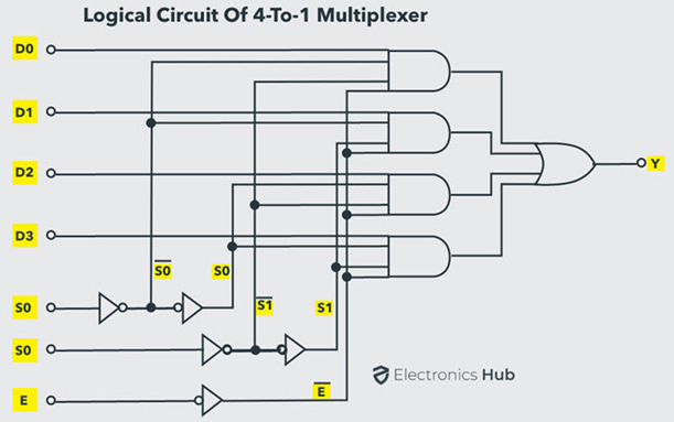
From the above truth table, we can write the output expressions as follows:
Y = S0 S1 D0 + S0 S1 D1 + S0 S1 D2 + S0 S1 D3
From the above expression of the output, a 4-to-1 multiplexer can be implemented by using basic logic gates. The below figure shows the logic circuit of 4:1 MUX which is implemented by four 3-inputs AND gates, two 1-input NOT gates, and one 4-inputs OR gate.
In this circuit, each data input line is connected as input to an AND gate and two select lines are connected as other two inputs to it. Additionally, there is also an Enable Signal. The output of all the AND gates are connected to inputs of OR gate in order to produce the output Y.
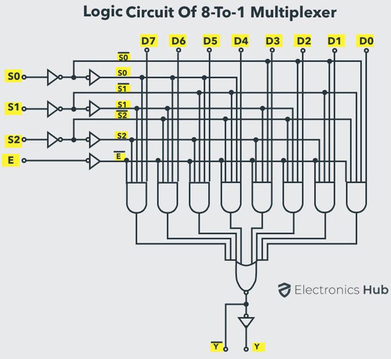
Quadruple 2:1 Multiplexer (8:1 multiplexer)
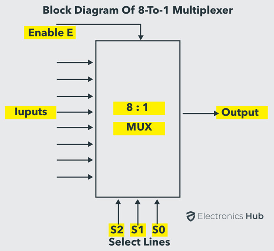
An 8-to-1 multiplexer consists of eight data inputs D0 through D7, three input select lines S0 through S2 and a single output line Y. Depending on the select lines combinations, multiplexer selects the inputs.
The below figure shows the block diagram of an 8-to-1 multiplexer with enable input that can enable or disable the multiplexer. Since the number data bits given to the MUX are eight, then 3 bits (23 = 8) are needed to select one of the eight data bits.
The truth table for an 8-to1 multiplexer is given below with eight combinations of inputs so as to generate each output corresponds to input.
For example, if S2= 0, S1=1 and S0=0 then the data output Y is equal to D2. Similarly the data outputs D0 to D7 will be selected through the combinations of S2, S1 and S0 as shown in below figure.
|
S0 |
S1 |
S2 |
D0 |
D1 |
D2 |
D3 |
D4 |
D5 |
D6 |
D7 |
Y |
|
0 |
0 |
0 |
0 |
X |
X |
X |
X |
X |
X |
X |
0 |
|
0 |
0 |
0 |
1 |
X |
X |
X |
X |
X |
X |
X |
1 |
|
0 |
0 |
1 |
X |
0 |
X |
X |
X |
X |
X |
X |
0 |
|
0 |
0 |
1 |
X |
1 |
X |
X |
X |
X |
X |
X |
1 |
|
0 |
1 |
0 |
X |
X |
0 |
X |
X |
X |
X |
X |
0 |
|
0 |
1 |
0 |
X |
X |
1 |
X |
X |
X |
X |
X |
1 |
|
0 |
1 |
1 |
X |
X |
X |
0 |
X |
X |
X |
X |
0 |
|
0 |
1 |
1 |
X |
X |
X |
1 |
X |
X |
X |
X |
1 |
|
1 |
0 |
0 |
X |
X |
X |
X |
0 |
X |
X |
X |
0 |
|
1 |
0 |
0 |
X |
X |
X |
X |
1 |
X |
X |
X |
1 |
|
1 |
0 |
1 |
X |
X |
X |
X |
X |
0 |
X |
X |
0 |
|
1 |
0 |
1 |
X |
X |
X |
X |
X |
1 |
X |
X |
1 |
|
1 |
1 |
0 |
X |
X |
X |
X |
X |
X |
0 |
X |
0 |
|
1 |
1 |
0 |
X |
X |
X |
X |
X |
X |
1 |
X |
1 |
|
1 |
1 |
1 |
X |
X |
X |
X |
X |
X |
X |
0 |
0 |
|
1 |
1 |
1 |
X |
X |
X |
X |
X |
X |
X |
1 |
1 |
From the above truth table, the Boolean equation for the output is given as:
Y = S0 S1 S2 D0 + S0 S1 S2 D1 + S0 S1 S2 D2 + S0 S1 S2 D3 + S0 S1 S2 D4 + S0 S1 S2 D5 + S0 S1 S2 D6 + S0 S1 S2 D7
From the above Boolean equation, the logic circuit diagram of an 8-to-1 multiplexer can be implemented by using 8 AND gates, 1 OR gate and 7 NOT gates as shown in below figure. In the circuit, when enable pin is set to one, the multiplexer will be disabled and if it is zero, then select lines will select the corresponding data input to pass through the output.
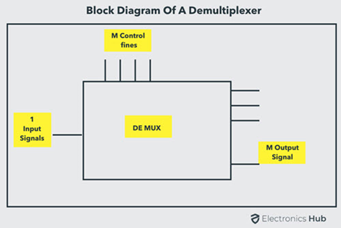
Demultiplexers:
Demultiplexer means one to many. A demultiplexer is a circuit with one input and many outputs. By applying control signal, we can steer any input to the output. Few types of demultiplexer are 1-to 2, 1-to-4, 1-to-8 and 1-to 16 demultiplexer.
Following figure illustrate the general idea of a demultiplexer with 1 input signal, m control signals, and n output signals.
1-to-4 Demultiplexer
The 1-to-4 demultiplexer has 1 input bit, 2 control or select bits, and 4 output bits. An example of 1-to-4 demultiplexer is IC 74155. The 1-to-4 demultiplexer is shown in figure below-

The input bit is labelled as Data D. This data bit is transmitted to the selected output lines, which depends on the values of A and B, the control or Select Inputs.
When A B = 0 1 , the second AND gate from the top is enabled while other AND gates are disabled. Therefore, data bit D is transmitted to the output Y1, giving Y1 = Data.
If D is LOW, Y1 is LOW. If D is HIGH, Y1 is HIGH. The value of Y1 depends upon the value of D. All other outputs are in low state.
If the control input is changed to A B = 1 0 , all the gates are disabled except the third AND gate from the top. Then, D is transmitted only to the Y2 output, and Y2 = Data.
Implementation using decoder, encoders:
1. Encoders –
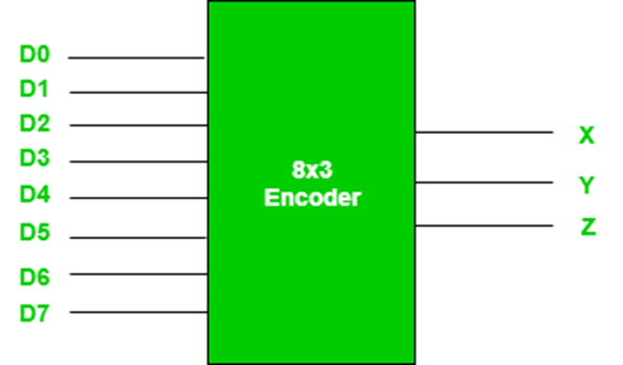
An encoder is a combinational circuit that converts binary information in the form of a 2N input lines into N output lines, which represent N bit code for the input. For simple encoders, it is assumed that only one input line is active at a time.
Octal to binary encoder
As an example, let’s consider Octal to Binary encoder. As shown in the following figure, an octal-to-binary encoder takes 8 input lines and generates 3 output lines.
Truth Table –
|
D7 |
D6 |
D5 |
D4 |
D3 |
D2 |
D1 |
D0 |
X |
Y |
Z |
|
0 |
0 |
0 |
0 |
0 |
0 |
0 |
1 |
0 |
0 |
0 |
|
0 |
0 |
0 |
0 |
0 |
0 |
1 |
0 |
0 |
0 |
1 |
|
0 |
0 |
0 |
0 |
0 |
1 |
0 |
0 |
0 |
1 |
0 |
|
0 |
0 |
0 |
0 |
1 |
0 |
0 |
0 |
0 |
1 |
1 |
|
0 |
0 |
0 |
1 |
0 |
0 |
0 |
0 |
1 |
0 |
0 |
|
0 |
0 |
1 |
0 |
0 |
0 |
0 |
0 |
1 |
0 |
1 |
|
0 |
1 |
0 |
0 |
0 |
0 |
0 |
0 |
1 |
1 |
0 |
|
1 |
0 |
0 |
0 |
0 |
0 |
0 |
0 |
1 |
1 |
1 |
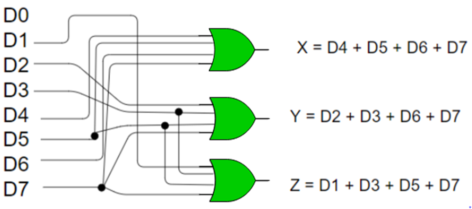
As seen from the truth table, the output is 000 when D0 is active; 001 when D1 is active; 010 when D2 is active and so on.
Implementation –
From the truth table, the output line Z is active when the input octal digit is 1, 3, 5 or 7. Similarly, Y is 1 when input octal digit is 2, 3, 6 or 7 and X is 1 for input octal digits 4, 5, 6 or 7. Hence, the Boolean functions would be:
X = D4 + D5 + D6 + D7
Y = D2 +D3 + D6 + D7
Z = D1 + D3 + D5 + D7
Hence, the encoder can be realised with OR gates as follows:
Decoders:
A decoder does the opposite job of an encoder. It is a combinational circuit that converts n lines of input into 2n lines of output.
3 to 8 line decoder
Truth Table –
|
X |
Y |
Z |
D0 |
D1 |
D2 |
D3 |
D4 |
D5 |
D6 |
D7 |
|
0 |
0 |
0 |
1 |
0 |
0 |
0 |
0 |
0 |
0 |
0 |
|
0 |
0 |
1 |
0 |
1 |
0 |
0 |
0 |
0 |
0 |
0 |
|
0 |
1 |
0 |
0 |
0 |
1 |
0 |
0 |
0 |
0 |
0 |
|
0 |
1 |
1 |
0 |
0 |
0 |
1 |
0 |
0 |
0 |
0 |
|
1 |
0 |
0 |
0 |
0 |
0 |
0 |
1 |
0 |
0 |
0 |
|
1 |
0 |
1 |
0 |
0 |
0 |
0 |
0 |
1 |
0 |
0 |
|
1 |
1 |
0 |
0 |
0 |
0 |
0 |
0 |
0 |
1 |
0 |
|
1 |
1 |
1 |
0 |
0 |
0 |
0 |
0 |
0 |
0 |
1 |
Implementation –
D0 is high when X = 0, Y = 0 and Z = 0. Hence,
D0 = X’ Y’ Z’
Similarly,
D1 = X’ Y’ Z
D2 = X’ Y Z’
D3 = X’ Y Z
D4 = X Y’ Z’
D5 = X Y’ Z
D6 = X Y Z’
D7 = X Y Z
Hence,

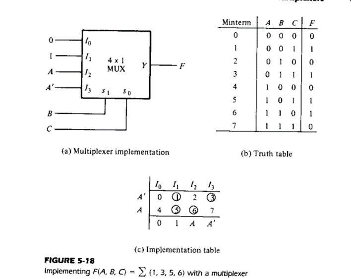
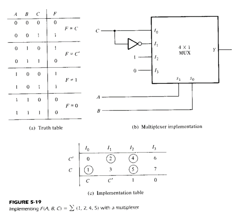
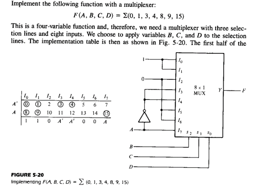
Boolean Function Implementation
Figures shows various Boolean function implementation