Automation in process control 5th Module
DIGITAL–TO-ANALOG CONVERTERS:
V-F, and F-V converters, performance specifications, D-A conversion techniques (R-2R & binary weighted) multiplying DACapplications. A-D conversion techniques (flash, successive approximation, single slope, dual slope), over sampling converters.
The functionof a voltage-to-frequency converter (VFC) is to accept an analog input vI and generatea pulse trainwith frequency,
fO = kvI
where k is the VFC sensitivity, in hertz per volt. As such, the VFC provides a simple form of analog-to-digital conversion.
Theprimary reason for this type of conversion is that a pulse train can be transmitted and decoded much more accurately than an analog signal, especially if the transmission path is long and noisy.
If electrical isolation is also desired, it can be accomplished without loss of accuracy using inexpensive optocouplers or pulse transformers. Moreover, combining a VFC with a binary counter and digital readout provides a low-cost digital voltmeter.
VFCs usuallyhave more stringent performance specifications than VCOs. Typicalrequirements are:
· wide dynamic range (four decadesor more),
· the ability to operate to relatively high frequencies (hundreds of kilohertz, or higher),
· Low linearity error (less than 0.1% deviationfrom the straightline going from zero to the fullscale),
· highscale-factor accuracy and stability with temperature and supply voltage.
The output waveform, on the other hand, is of secondary concern as long as its levels are compatible with standard logic signals. VFCs fall into two categories: wide-sweep multivibrators and charge-balancing VFCs
Wide-Sweep Multivibrator VFC
These circuits are essentially voltage-controlled astable multivibrators designed with VFC performance specifications in mind.
A popular product in this categoryis the AD537 The op amp and Q1 form a bufferV-I converter that convertsvI to the current drive iI for the CCO according to iI =vI /R.
The CCO(current controlled oscillator) parameters have been chosen so that fO = iI /(10C), or
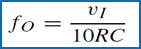
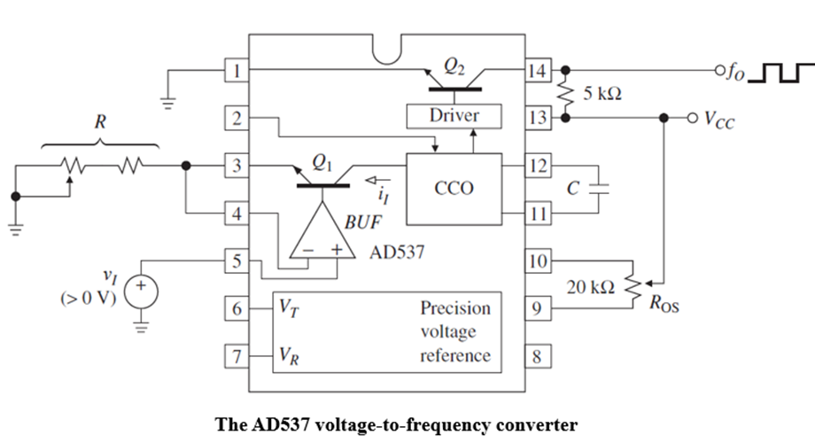
This relationship holds fairly accurately over a dynamic range of at least four decades, up to a full-scale current of 1 mAand a full-scale frequency of 100 kHz. For instance, with C = 1 nF, R = 10 kΩ, and VCC = 15 V, varying vI from 1 mV to 10 V variesiI from 0.1 μA to 1 mA and fO from 10 Hz to 100 kHz.
The device can also function as a current-to-frequency converter (CFC) if we make the control current flow out of the inverting input node. For instance, grounding pin 5 and replacing R by a photodetector diode current sink will convertlight intensity to frequency.
The AD537 also includes an on-chip precision voltage reference to stabilize the CCO scale factor. This yields a typical thermal stability of 30 ppm/◦C. To further enhance the versatility of the device, two nodes of the reference circuitry are made available to the user,namely, VR and VT .
Figure also shows anotheruseful feature of the AD537, namely, the ability to transmit information over a twistedpair. This pair servesthe dual purposeof supplying powerto the device and carryingfrequency data in the form of current modulation.
Charge-Balancing VFC
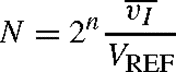
The charge-balancing technique supplies a capacitor with continuous charge at a rate that is linearly proportional to the input voltage vI , while simultaneously pullingdiscrete charge packetsout of the capacitor at a rate fO such that the net charge flow is always zero. The result is fO = kvI
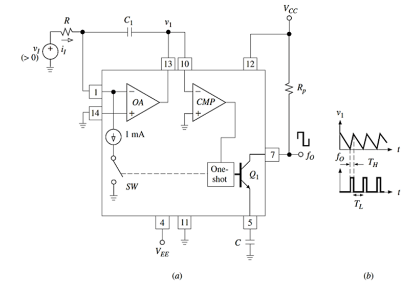
OA converts vI to a current i1 = v1/R flowing into the summingjunction; the valueof R is chosensuch that we always have i I < 1 mA. With SW open, iI flows into C1 and causes v1 to ramp downward.
As soon as v1 reaches 0 V, CMP fires and triggers a precision one-shot that closes SW and turns on Q1 for a time interval TH set by C. The one-shot, whose details have been omitted for simplicity, uses a threshold of 7.5 V and a charging current of 1 mA to give
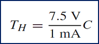
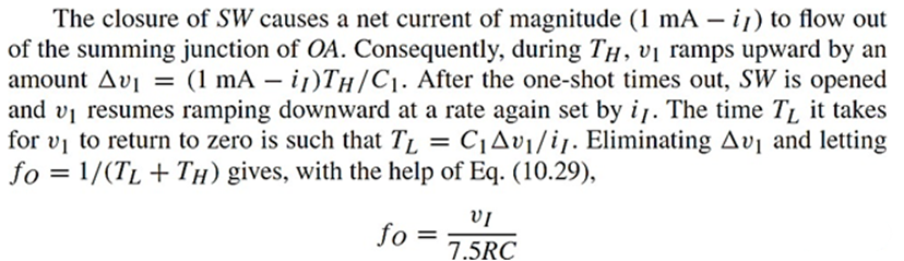

The absence of C1 from the above equationsindicates that the tolerance and drift of this capacitor are not critical, so its value can be chosen arbitrarily. However, for optimum performance, the data sheets recommend using the value of C1 that yields v1∼= 2.5 V. C, on the other hand, so it must be a low-drift type, such as NPO ceramic. If C and R have equal but opposing thermal coefficients, the overall drift can be reduced to as little as 20 ppm/◦C. For accurate operationto low values of vI , the input offsetvoltage of OA must be nulled
Frequency-to-Voltage Conversion
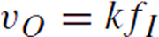
The frequency-to-voltage converter (FVC)performs the inverse operation, namely, it accepts a periodic waveform of frequency fI and yields an analog output voltage:
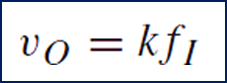
where k is the FVC sensitivity, in volts per hertz. FVCs find application as tachometers in motorspeed control and rotational measurements. Moreover, they are used in conjunction with VFCs to convert the transmitted pulse train back to an analog voltage
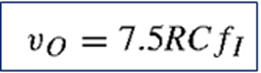
A charge balancing VFC can easily be configured as an FVC by applying the periodic input to the comparator and deriving the output from the op amp, which now has the resistance R in the feedback path (see fig)
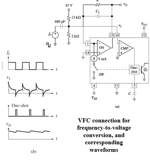
The input signal usually require proper conditioning to produce a voltage with reliable zero crossing for CMP. Shown in the figure is a high pass network to accommodate inputs of the TTL and CMOS type.
On each negative spike of v1, CMP triggers the one-shot, closing SW and pulling 1 mA out of C1 for a duration TH. In response to this train of current pulses, vO builds up until the current pulled out of the summingjunction of OA in1-mA packets is exactly counterbalanced by that injected by vovia R continuously, or f I x 10-3 x TH = vo/R
olving for Vo gives
The value of C is determined on the basis of a maximum duty cycle of 25 percent, as discussed earlier, while R now establishes the full-scale value of vO. As in the VFC case, the input offset voltage of OA should be nulled to avoid degrading the conversion accuracy at the lowend of the range.
D-A CONVERSION TECHNIQUES
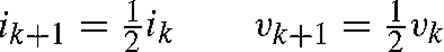
Weighted Resistor DAC
The functions required to implement an n-bit DAC are n switch and n binary- weighted variables to synthesize the terms bk2−k , k = 1, 2, . . . , n; moreover, we need an n-input summer,and a reference
The DAC of Fig uses an op amp to sum n binary-weighted currents derived from VREF via the current-scaling resistances 2R, 4R, 8R, . . . , 2n R. Whether the current ik = VREF/2kR appears in the sum depends on whether the corresponding switch is closed (bk = 1) or open (bk = 0). Writing vO = −R f iO gives:

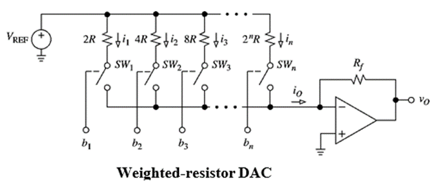
The conceptual simplicity of the weighted-resistor DAC is offset by two drawbacks, namely, the nonzero resistances of the switches, and a spread in the current-setting resistances that increases exponentially with n.
The effect of switch resistances is to disrupt the binary-weighted relationships of the currents, particularly in the most significant bit positions, where the current-setting resistances are smaller.
These resistances can be made sufficiently large to swamp the switch resistances; however, this may result in unrealistically large resistances in the least significant positions.
For instance, an 8-bit DAC requires resistances ranging from 2R to 256R. The difficulty in ensuring accurate ratios over a range this wide, especially in monolithic form, restricts the practicality of resistor-weighted DACs below 6 bits.
R-2R Ladder DAC
Most DAC architectures are based on the popularR-2R ladder depictedin Fig.
The currentflowing downward, away from each node, is equal to the current flowing toward the right; moreover,twice this currententers the node from the left. The currents and, hence, the node voltagesare binary-weighted,
where k = 1, 2, . . . , n − 1.
With a resistance spread of only 2-to-1, R-2R ladders can be fabricated monolithically to a high degree of accuracy and stability. Thin-film ladders, fabricated by deposition on the oxidized silicon surface, lend themselves to accurate laser trimming for DACs with n ≥ 12. For DACS with a lower number of bits, diffused or ion-implanted ladders are often adequate. Depending on how the ladder is utilized, different DAC architectures result.
A-D CONVERSION TECHNIQUES
Successive-Approximation Converters (SA ADCs)
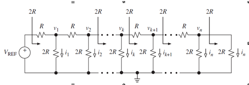
This technique uses the register as a successive-approximation register (SAR) to find each bit by trial and error. Starting from the MSB, the SAR inserts a trial 1 and then interrogates the comparator to find whether this causes vO to rise above vI .
If it does, the trial bit is changed back to 0; otherwise, it is left as 1. The procedure is then repeated for all subsequent bits, one bit at a time.
Figure illustrates how a 10.8-V input is converted to a 4-bit code with VFSR = 16 V. The analog range, in volts, is at the left, and the digital codes at the right. To ensure correct results, the DAC output must be offset by −12 LSB, or −0.5 V in our example.
The conversion takes place as follows:
Following the arrival of the START command, the SAR sets b1 to 1 with all remaining bits at 0 so that the trial code is 1000. This causes the DAC to output vO = 16 (1 × 2−1 + 0 × 2−2 + 0 × 2−3 + 0 × 2−4) − 0.5 = 7.5 V. At the end of clock period T1, vO is compared against vI , and since 7.5 < 10.8, b1 is leftat 1.
At the beginning of T2, b2 is set to 1, so the trial code is now 1100 and vO = 16(2−1 +2−2) − 0.5 = 11.5 V. Since 11.5 >10.8, b2 is changedback to 0 at the end of T2.
At the beginning of T3, b3 is set to 1, so the trial code is 1010 and vO =10 − 0.5 = 9.5 V. Since 9.5 < 10.8, b3 is left at 1.
At the beginning of T4, b4 is set to 1, so the trial code is 1011 and vO= 11 − 0.5 = 10.5 V. Since 10.5 < 10.8, b4 is left at 1. Thus, when leaving T4, the SAR has generated the code 1011, which ideally corresponds to 11 V. Note that any voltage in the range 10.5 V < vI < 11.5 V would have led to the same code.
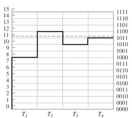
Figure shows an actual implementation using the Am2504 SAR and the Am6012 bipolar DAC
SA ADCs are available from a variety of sources and in a wide range of performance characteristics and prices. Conversion times typically range from under 1 μs for the faster 8-bit units to tens of microseconds for the high- resolution (n ≥14) types. SA ADCs equipped with an on-chip SHA are referred to as sampling ADCs.A popular example is the AD1674 12-bit, 100-kilosamples per second (ksps) SA ADC.
Flash Converters
The circuit of Figure uses a resistor string to create 2n − 1 reference levels separated from each other by 1 LSB, and a bank of 2n − 1 high- speed latched comparators to simultaneously compare vI against each level.
Note that to position the analog signal range properly, the top and bottom resistors must be 1.5R and 0.5R, as shown. As the comparators are strobed by the clock, the ones whose reference levels are below vI will output a logic 1, and the remaining ones a logic 0.
The result, referred to as a bar graph, or also as a thermometer code, is then converted to the desired output code b1 . . . bn by a suitable decoder, such as a priority encoder.
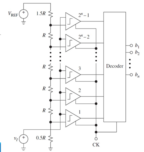
Since input sampling and latching take place during the first phase of the clock period, and decoding duringthe second phase, the entire conversion takes only one clock cycle,so this ADC is the fastest possible.
Aptly called a flash converter, it is used in high-speed applications, such as video and radar signal processing, where conversion rates on the order of millions of samples per second (Msps) are required, and SA ADCs are generally not fast enough. The high-speed and inherent-sampling advantages of flash ADCs are offset by the fact that 2n−1 comparators are required.
For instance, an 8-bit converter requires 255 comparators. The exponential increase with n in die area, power dissipation, and stray input capacitance makes flash converters impractical for n > 10.
Flash ADCs are available in bipolar or in CMOS technology, with resolutions of 6, 8, and 10 bits, sampling rates of tens to hundreds of Msps, depending on resolution, and power dissipation ratings on the order of 1 W or less.
Dual-slope ADC
Integrating-type converters perform A-D conversion indirectly by converting the analog input to a linear function of time and hence to a digital code. The two most common converter types are the charge- balancing and dual-slope ADCs.
As shown in the functional diagram of Fig, a dual-slope ADC, also called a dual-ramp ADC, is based on a high- input-impedance buffer, a precision integrator, and a voltage comparator.
The circuit first integrates the input signal vI for a fixed duration of 2n clock periods, and then it integrates an internal reference VREF of opposite polarity until the integrator output is brought back to zero.
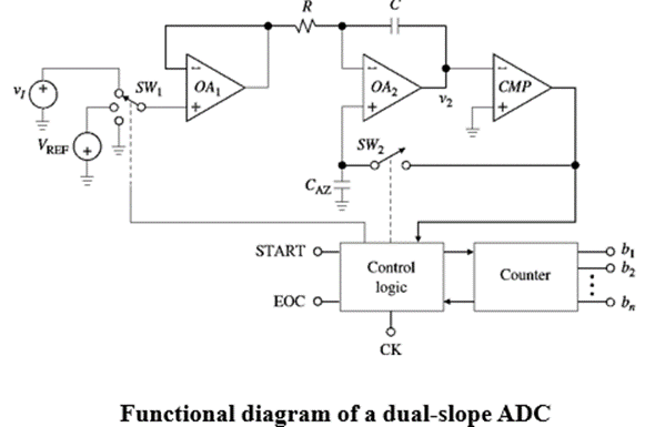
The number N of clock cycles required to return to zero is proportional to the value of vI averaged over the integration period. Consequently, N represents the desired output code.
With reference to the waveform diagram of Fig., following is a detailed description of how the circuit operates.
Prior to the arrival of the START command, SW1 is connected to ground and SW2 closes a loop around the integrator-comparator combination. This forces the autozero capacitance CAZ to develop whatever voltage is needed to bring the output of OA2 right to the comparator’s threshold voltage and leave it there. This phase, referred to as the autozero phase, provides simultaneous compensation for
the input offset voltages of all three amplifiers. During the subsequent phases, when SW2 opens, CAZ acts as an analog memory to hold the voltage required to keep the net offset nulled.
At the arrival of the START command, the control logic opens SW2, connects SW1 to vI (which we assume to be positive), and enables the counter, starting from zero. This phase is called the signal integrate phase. As the integrator ramps downward, the counter counts until, 2n clock periods later, it overflows. This marks the end of the current phase.
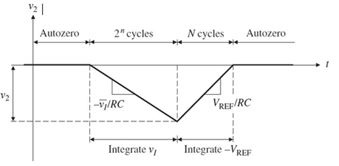
As the overflow condition is reached, the counter resets automatically to zero and SW1 is connected to −VREF, causing v2 to ramp upward. This is called the deintegrate phase. Once v2 again reaches the comparator threshold, the comparator fires to stop the counter and issues an EOC command. The accumulated count N is such that CΔv2 = (VREF/R)NTCK. Since CΔv2 is the same during the two phases, we get