Micro and Smart System Technology 1st Module
Micro-Electro-Mechanical Systems (MEMS) is the integration of mechanical elements, sensors, actuators, and electronics on a common silicon substrate through micro fabrication technology.
Feynmans vision - As Nobel Laureate physicist Richard Feynman noted in his lectures, the laws of science as we know them today do not preclude miniaturization, and there is sufficient room at the bottom. It is only a question of developing the requisite technologies and putting them together to make it all happen.
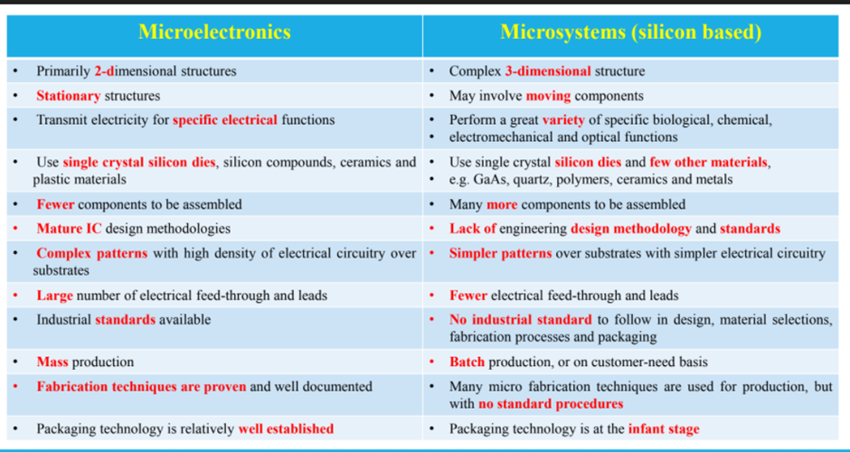
Microsystems versus MEMS
Why Miniaturization?
✓A microsystem is a system that integrates, on a chip or in a package, one or more of many things: sensors, actuators, electronics, computation, communication, control, power generation, chemical processing, biological reactions, and more.
✓Miniaturization is essential in achieving this level of integration of a disparate array of components.
✓There is no doubt that the functionality of such an integrated system will not only be far superior to any other engineered system that we know at the macroscale but will also achieve things beyond those achievable by macrosystems.
Smaller systems tend to move more quickly than larger systems because of lower inertia of the mass.
❑ The minute sizes of small devices encounter fewer problems in thermal distortion and vibration
❑ Their minute size makes them particularly suitable for applications in medicine and surgery and in microelectronic assemblies in which miniaturized tools are necessary.
❑ Less material requirements mean low cost of production and transportation.
❑ Smaller size of the systems means less space requirements. This allows the packaging of more functional components in a single device.
Microfabrication –
❑Microsystems technology emerged as a new discipline based on the advances in integrated circuit (IC) fabrication
processes, by which sensors, actuators and control functions were co-fabricated in silicon.
❑The concepts and feasibility of more complex microsystems devices have been proposed and demonstrated for
applications in such varied fields as microfluidics, aerospace, automobile, biomedical, chemical analysis, wireless
communications, data storage, and optics.
❑In microsystems, miniaturization is achieved by a fabrication approach similar to that followed in ICs, commonly
known as micromachining.
❑The Machining here does not refer to conventional approaches (such as drilling, milling, etc.) used in realizing
macro-mechanical parts, although the objective is to realize such parts.
Silicon micromachining has been the key factor in the fast progress of microsystems in the last decade of the 20th century. This is the
fashioning of microscopic mechanical parts out of silicon substrates and more recently other materials.
❑ Bulk micromachining, which involves carving out the required structure by etching out the silicon substrate, is the commonly used method.
❑ Surface micromachining is an alternate micromachining approach. It is based on
patterning layers deposited on the surface of silicon or any other substrate. This
approach offers the attractive possibility of integrating the micromachined device with
microelectronics patterned and assembled on the same wafer.
Smart Materials, Structures & Systems
The area of smart material systems has evolved from the unending quest of mankind to mimic systems of natural origin. The objective of such initiatives is to develop technologies to produce nonbiological systems that achieve optimum functionality as observed in natural biological systems and emulate their adaptive capabilities by an integrated design approach.
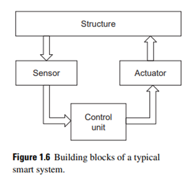
In the present context, a smart material is one whose electrical, mechanical, or acoustic properties or whose structure, composition, or functions change in a specified manner in response to some stimulus from the environment. In a similar way, one may envisage smart structures that require the addition of properly designed sensors, actuators, and controllers to an otherwise ‘‘dumb’’ structure (see schematic in Figure 1.6).
As smart materials systems should mimic naturally occurring systems, the general requirements expected from these nonbiological systems include:
1. Full integration of all functions of the system.
2. Continuous health and integrity monitoring.
3. Damage detection and self-recovery.
4. Intelligent operational management.
5. High degrees of security, reliability, efficiency and sustainability.
Besides ‘‘smart system’’ or ‘‘smart material,’’ another widely used term is smart structure. One distinctive feature of smart structures is that actuators and sensors can be embedded at discrete locations inside the structure without affecting the structural integrity of the main structure. An example is the embedded smart structure in a laminated composite structure.
Integrated Microsystems
Integrated microsystems can be classified into three major groups as follows:
1. Micromechanical structures: These are non-moving structures, such as microbe-ams and microchannels.
2. Microsensors: These respond to physical and chemical signals (such as pressure, acceleration, pH, glucose level, etc.) and convert them to electrical signals
3. Microactuators: These convert electrical or magnetic input to mechanical forms of energy (e.g. resonating beams, switches, and micropumps)
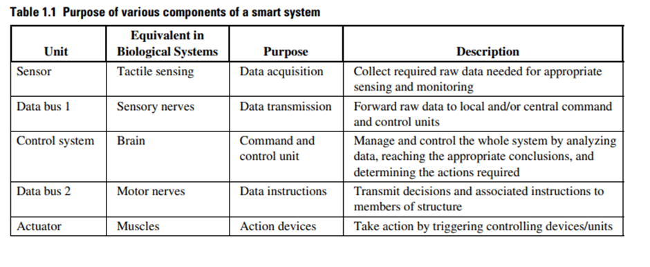
Microsystems integrate sensors, actuators and electronics to provide some useful function. The ADXL50, which was released in 1991 and was Analog Devices’ first commercial device, is an excellent example of such a microsystem. The block diagram of this system is shown in Figure 1.8
This microsystem is based on a surface micro-machining technology with sensing electronics integrated on the same chip as the accelerometer. Here, the accelerometer is a sensor that responds to the acceleration or deceleration and gives an output voltage to the control circuit, which in turn triggers an actuator to deploy the airbag during a crash, so that the persons seated in the front seat are protected from crashing into the front windshield or the dashboard
Micromechanical Structures Micromachining is used commercially to produce channels for microfluidic devices and also to fabricate systems referred to as ‘‘labs on a chip’’ for chemial analysis and analysis of biomedical materials. Usually such channels are made on plastics or glass substrates. Figure 1.9 (a) shows one such device reported in the literature. Micro-machining is also used to make a variety of mechanical structures. Figure 1.9 (b) shows an SEM image of a silicon nanotip fabricated [9] using a ‘‘bulk micromachining’’ process. Such microtips find applications in atomic force microscopy (AFM) technology and field emission array for futuristic vacuum electron devices capable of operation in terahertz frequency range
Microsensors
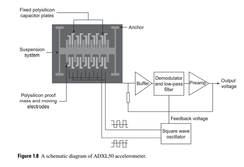
Several micro machined sensors have evolved over the last two decades. Among them the pressure sensors occupy almost 60% of the market. A schematic isometric cut-away view of a piezoresistive pressure sensor die is shown in Fig. 1.10 (a). Here, we can see the four pressure-sensitive resistors (piezoresistors) integrated on a micromachined silicon diaphragm. Micromachined accelerometer is yet another device which has received considerable attention from the aerospace, automobile, and biomedical industries. Figure 1.10 (b) shows a schematic cross-sectional view of one such device. The seismic mass responds to acceleration and deflects, thus bringing about a change in the capacitance between the mass and the fixed electrodes. The change in capacitance is a measure of the displacement, which in turn depends upon the acceleration.
Microactuators
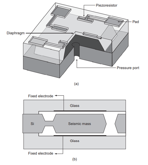
In this we have two examples of actuators are presented to highlight the wide range of applications of microactuators. First, a schematic diagram of the electrostatically actuated bulk micromachined silicon micropump is shown in Figure 1.11.
The diaphragm deflects upward when an actuation voltage is applied as shown and the inlet check valve opens due to a fall in chamber pressure, thereby letting in the fluid flow into the pump chamber. When the actuation voltage drops to zero, the diaphragm moves back to its equilibrium position. As the chamber is now full of fluid, the pressure inside is higher than that outside. This forces the inlet valve to close and the outlet valve to open, thus letting the fluid flow out.
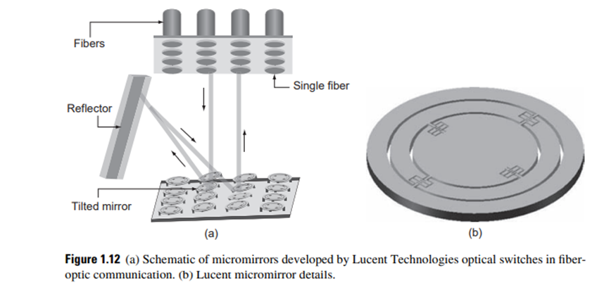
The second example is the famous electrostatically actuated micromirror array consisting of tiny mirrors as shown in Figure 1.12.
Each mirror is 0.5 mm in diameter, about the size of the head of a pin. Mirrors rest 1 mm apart and all 256 mirrors are fabricated on a 2.5 cm square piece of silicon. The figure on the left-hand side shows how the tilted mirrors switch the optical signals from one fiber to another fiber.
Thus, there is no need of making an optoelectronic conversion. This arrangement gives 100-fold reduction in power consumption over electronic switches
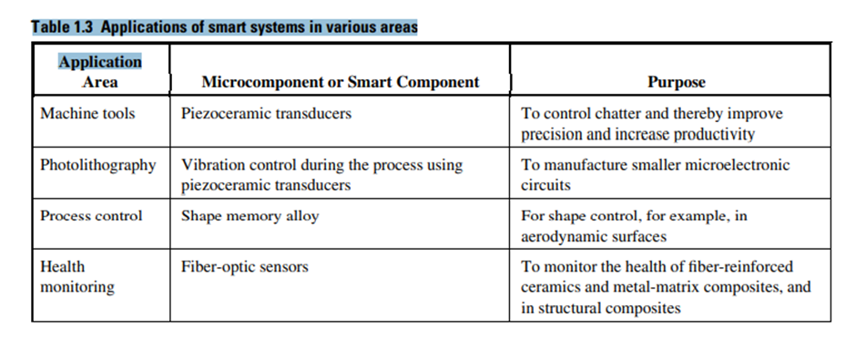
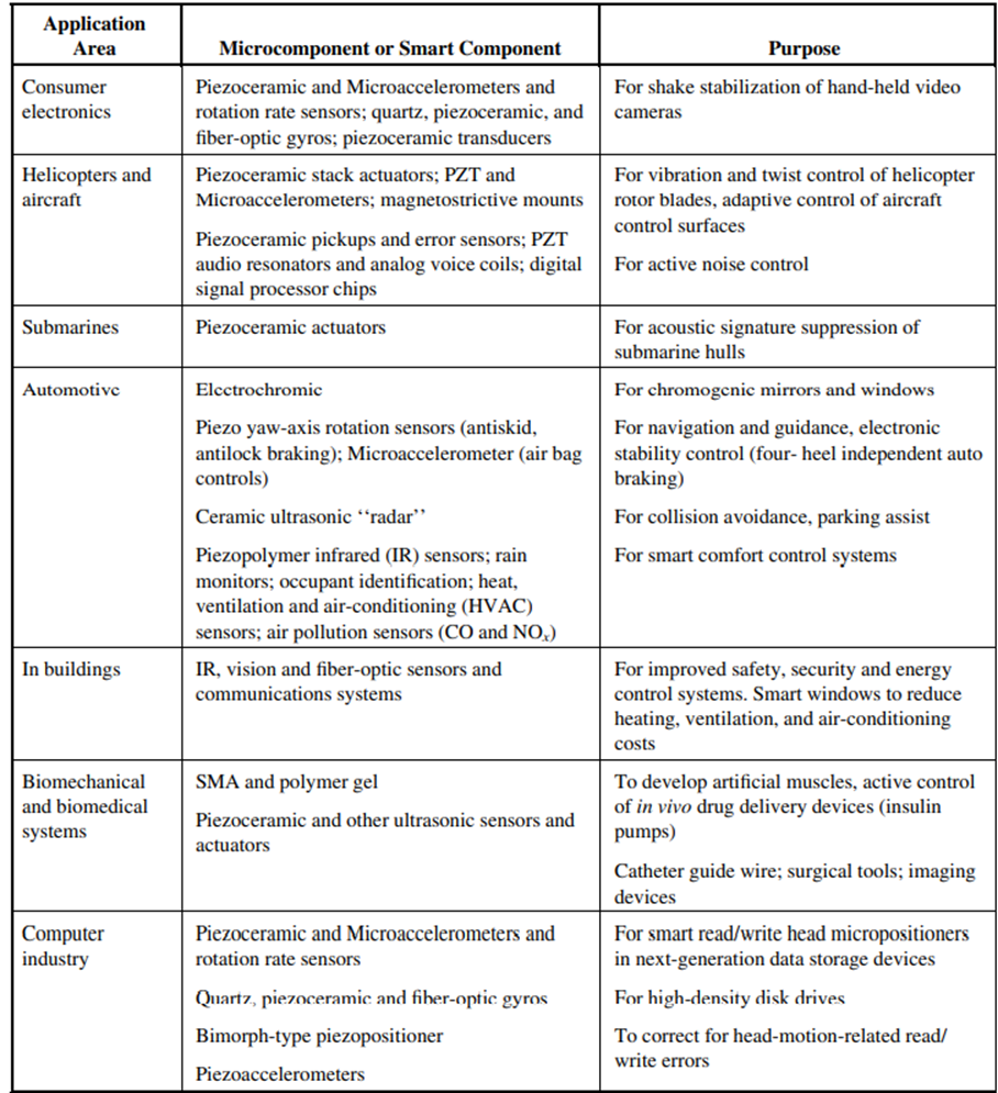
APPLICATIONS OF SMART MATERIALS AND MICROSYSTEMS
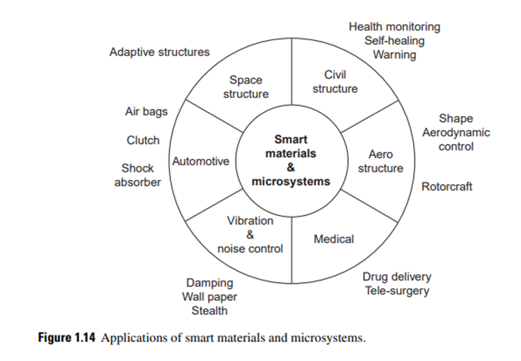
The area of smart materials and structures is an interdisciplinary field bridging the gap between science and technology and combining knowledge in physics, mathematics, chemistry, material science, electrical and mechanical engineering. Through such a technology, we can build safer cars, more comfortable airplanes, self-repairing water pipes, etc. Smart structures can help us to monitor and control the environment better and to increase the energy efficiency of devices. The applications of microsystems encompass the entire range of civilian, defense, automobile, biomedical, and consumer devices used in day-to-day life.