
Micro and Smart System Technology 3rd Module
Silicon as a material for micromachining
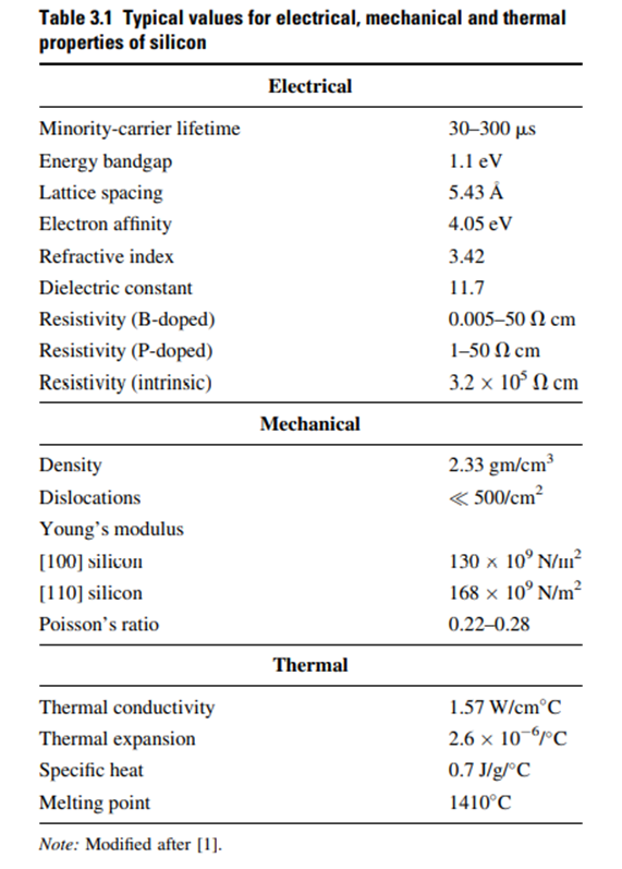
The most commonly used semiconductor material for microsystems applications is silicon, since it can be modified to alter its electrical, mechanical, and optical properties. Silicon and its compounds are the key materials used for micromachining and fabrication technology, for these materials have reached a state of maturity. In addition, silicon has many desirable mechanical properties that can be exploited in microsystems applications. Some properties of silicon relevant in microsystems are shown in fig
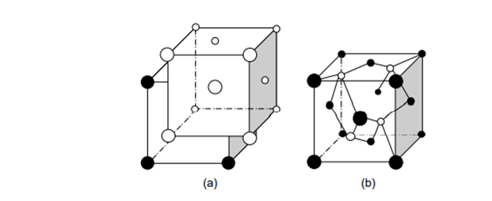
Silicon crystals are made up of two interpenetrating face-centered cubic (FCC) cells. In an FCC cell, atoms are located at the eight corners of the cubic lattice structure and one atom at the center of each face. Because of interpenetration of two FCC unit cells, the unit Silicon crystals are made up of two interpenetrating face-centered cubic (FCC) cells. In an FCC cell, atoms are located at the eight corners of the cubic lattice structure and one atom at the center of each face. Because of interpenetration of two FCC unit cells, the unit cell of silicon crystal contains four more atoms.
Therefore, the silicon unit cell shown in Fig. 3.2 has 18 atoms with eight atoms at the corners, six atoms at the face centers, and four more atoms inside the unit cell (shown as hollow spheres) [2]. Atoms at the boundaries are shared between adjacent cells. A bulk silicon crystal may be considered as stacked layers of periodically repeating FCC unit cells
Silicon wafer preparation
Silicon is abundantly available in nature in the form of sand (SiO2) or quartz. It must be converted into high-purity single-crystal silicon (SCS) with impurity level less than 1 ppb (parts per billion) for use in semiconductor and microsystems devices. Sand (high-purity sand, commonly known as quartzite) is converted into high-purity SCS by the following series of processing steps.
Quartzite is refined chemically with carbon in an arc furnace at a very high temperature to obtain 90%–99% pure silicon. This material, usually known as metallurgical-grade silicon (MGS), is treated with hydrochloric acid to get trichlorosilane (SiHCl3). At room temperature trichlorosilane is in liquid form. Fractional distillation of SiHCl3 in a hydrogen atmosphere yields electronic-grade silicon (EGS). The polycrystalline EGS obtained by the above process is the basic material for the preparation of silicon wafers.
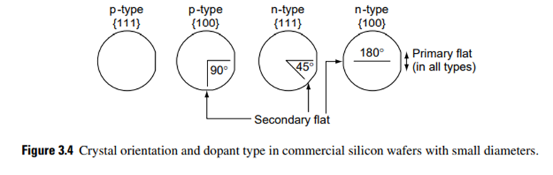
The surface of the single-crystal ingot thus obtained is ground to make it cylindrical. For ingots with diameter less than 800 (200 mm), one or more flat regions are ground along the length of the ingot to specify the crystal orientation and the type of dopant (Fig. 3.4). In manual processing, these flats are also useful in aligning masks with crystal directions during lithography.
Following this, circular wafers (thin sections of the crystal) are sliced off the ingot using a high-speed diamond saw. The thickness of a wafer depends on its diameter and ranges from 100 mm to about 1 mm. To produce perfectly flat, smooth, and damage-free surfaces, the wafers are first lapped to remove irregularities introduced during sawing. They are chemically etched and polished to a mirror finish and uniform thickness.
Thin Film Deposition Techniques
Chmical Vapor deposition
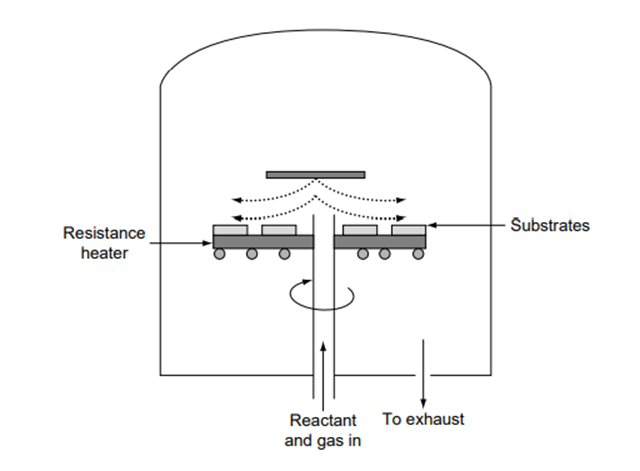
The CVD process involves convective heat and mass transfer and chemical reaction at the substrate surface. Even though the CVD process is more complex, it gives more effective control on the growth rate and the quality of deposited films. Most CVD processes involve low gas pressures (100–200 mtorr) [4]. The principle of operation involves the flow of a carrier gas with diffused reactants over large substrate surfaces.
The energy supplied by the heated surface triggers chemical reaction of the reactants, thus forming thin films over the surface of the substrates. The byproducts of chemical reaction are vented out. A typical CVD reaction chamber is shown in Fig. 3.7.
A CVD process that requires elevated temperature (700–800C) and near-atmospheric pressure is called atmospheric pressure chemical vapor deposition (APCVD). The lowpressure chemical vapor deposition (LPCVD) and plasma-enhanced chemical vapor deposition (PECVD) processes are used to achieve higher growth rates and better deposited film quality at lower temperatures.
The deposited film is usually uniform. Batch processing of stacked wafers is possible by this method
Parameters that significantly influence the rate of CVD are: 1. Temperature 2. Pressure of carrier gas 3. Velocity of gas flow 4. Distance along the direction of gas flow
Photolithography
Resists used in this approach are called photoresists. Depending upon their response to UV radiation, photoresists are classified as positive or negative photoresists. In a positive photoresist, the exposed region is removed after developing, while in a negative photoresist, the exposed region is retained after developing (Fig. 3.9).
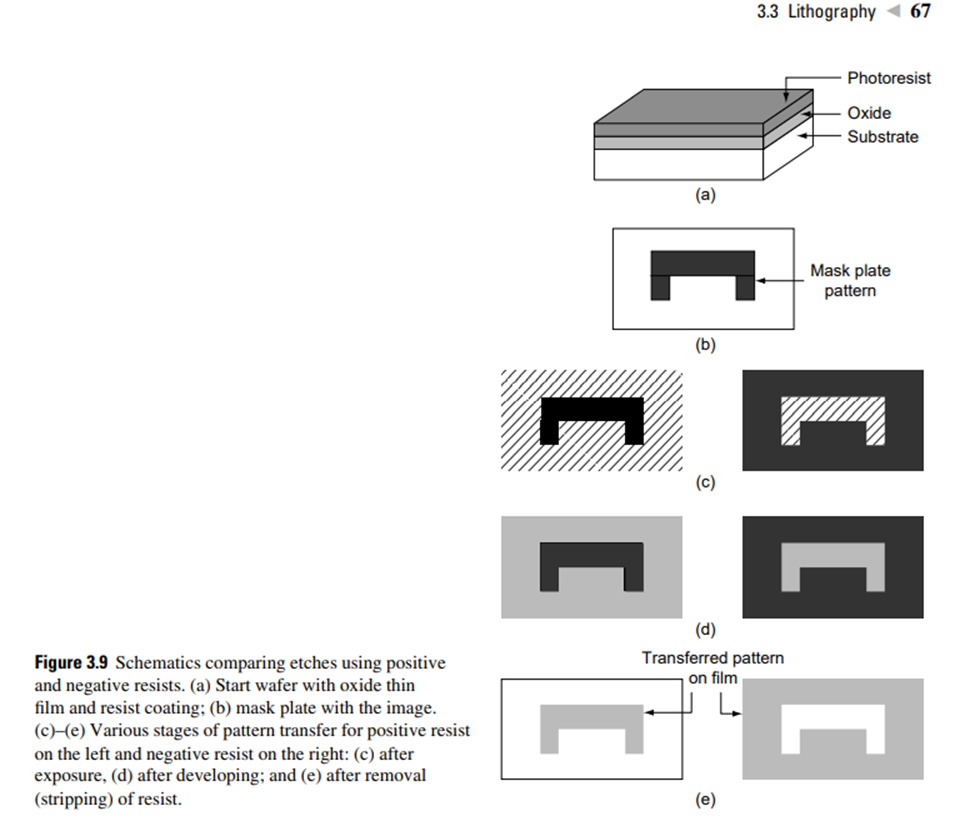
Some of the key processes involved in photolithography are the coating of resist, pattern transfer, and development. The resist material is entirely removed after an underlying layer is etched with the resist as the masking window.
1. Resist coating: A few drops of the resist materials are placed on a clean wafer. A high-speed (typically ranging from 2000 to 8000 rpm), high-acceleration spinner is used to produce a uniform coating of photoresist on the substrate surface.
2. Prebaking: Before transferring the pattern to the photoresist film, one must ensure that it sticks well to the surface. To improve adhesion of the film, the substrate is prebaked at 75C to 100C for about 10 minutes. This step removes organic solvents and releases stress in the film in addition to improving adhesion.
3. UV exposure: Pattern transfer by UV exposure is carried out using a mask aligner. For good results, the UV source should have proper intensity, directionality, spectral characteristics, and radiation uniformity across the exposed area.
4. Developing: After exposure, developing removes the softened portion of the photoresist. In positive resists, this removes the exposed region; in negative resists, it removes the unexposed region of the resist. The solvent system used for developing depends on the photoresist material.
5. Postbaking: Postbaking at 120C for about 20 minutes removes residual solvents, improves further adhesion, and toughens the remaining photoresist.
6. Etching: Etching removes unwanted material from the substrates through the windows opened by developed regions of the photoresist. This step transfers a pattern of the material layer on to the substrate. Details of this step are discussed in subsequent sections.
7. Photoresist stripping: After all process steps are performed for pattern transfer, the photoresist is removed by an organic solvent
Most pattern transfer required for microsystems can be done by photolithography. One of the limitation of this technique is its scalability to nanodevices.
Lift-Off Technique
The lift-off technique is used to define structural geometry on the substrate. The process steps involved in the lift-off technique are shown in Fig. 3.10.
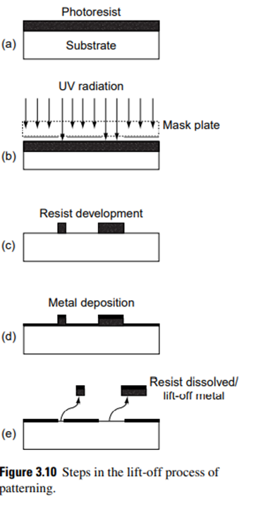
The resist is spin-coated, exposed to radiation through a suitable mask, and developed in a developer. At this stage, selected portions of resist remain on the surface, as shown in Fig. 3.10 (c), and this is hardened by postbaking.
A thin film of the required material is then deposited above this layer of the resist [Fig. 3.10 (d)]. The resist is dissolved in appropriate solvent that detaches the material on top of the resist as well, leaving the film in the position where the photoresist was removed during development [see Fig. 3.10 (e)].
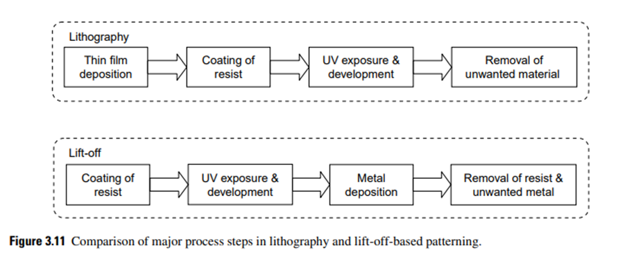
The unwanted material is ‘‘lifted off’’ while dissolving the photoresist. Unlike conventional lithography, in the lift-off process, a photoresist pattern is generated initially on the substrate instead of etching the unwanted material. Fig. 3.11 shows the key differences in process steps in these processes.
SILICON MICROMACHINING
Micromachining of silicon can be classified into bulk micromachining and surface micromachining
Bulk Micromachining
In bulk micromachining techniques, a significant amount of material is removed from the silicon wafer to form membranes, cantilever beams, different types of trenches, holes, and other types of structures. With bulk micromachining processes and wet chemical etchants, microstructures can be fabricated on SCS by undercutting the silicon wafer.
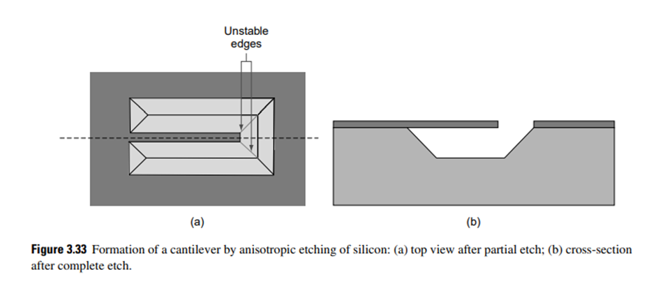
As an illustration, we describe the fabrication process steps to build a cantilever beam on a silicon wafer by bulk micromachining. A cantilever structure (Fig. 3.33) is realized by forming a beam fixed at one end and a cavity in the silicon substrate so that the other end can move freely. Obviously, the material of the beam must differ from the silicon substrate in which the cavity is formed. The most obvious material for cantilever beam is silicon dioxide (SiO2), which can be conveniently grown on native silicon by thermal oxidation.
Anisotropic etching is carried out to form a cavity in the silicon water. The steps involved are:
1. Grow a thick SiO2 layer on a silicon wafer.
2. Spin-coat the photoresist on SiO2 surface.
3. Carry out photolithography to define the cantilever geometry for oxide etch.
4. Etch out oxide in unwanted areas to form a cantilever beam and expose the silicon surface.
5. Do anisotropic etching to form a cavity in the silicon wafer
During the last step, a [111] plane is initially formed at all sides of the U-shaped trench. However, the convex corners thus formed (marked in Fig. 3.33) are not stable, as the atoms along this direction are not strongly bonded to other atoms underneath, and as a result are attacked by the etchant. As this process continues, the etch stops with the formation of a complete hollow pyramid underneath the rectangular etch window. This leaves the part made on the hard mask (SiO2) to remain as a cantilever
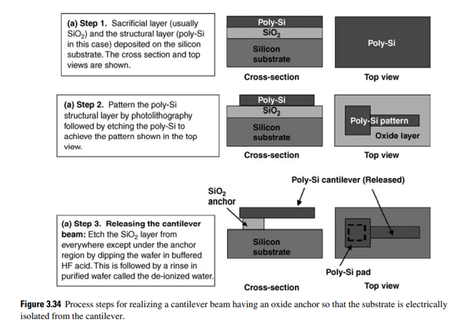
Surface Micromachining
Surface micromachined microsystem devices have three components: the sacrificial or spacer layer, the microstructure, and the insulator.
The basic steps involved in sacrificial layer technology for surface micromachining are illustrated in Fig. 3.34 by a surface micromachining technique used to realize a polysilicon cantilever beam using thermal oxide or deposited oxide as the sacrificial layer and anchor layer. Note that the polysilicon pad is larger than the width of the cantilever portion.
This ensures that the SiO2 anchor is not etched during release of the cantilever. Usually, etch holes are provided on wider structural layers to facilitate easy removal of sacrificial material from underneath. This sacrificial material removal (called the release step) is a very critical step in surface micromachining and is generally carried out after dicing into individual dies, particularly if one is planning to package.
Yet when large-area cantilever beams are formed by micromachining, they tend to deflect downward due to surface tension induced by trapped liquid droplets attached to the substrate or isolation layer during final rinsing and drying, a phenomenon is known as stiction (short form for static friction).
SPECIALIZED MATERIALS FOR MICROSYSTEMS
Polymers
Epoxy resins and adhesives are routinely used in microsystems packaging. Some of the well-established applications of polymers in the area of microsystems are:
1. Etch-stop layers for creating desired patterns for photolithography.
2. As prime molds with desired geometry of microcomponents in the LIGA (see Section 3.9.3.1) process.
3. Conductive polymers as organic semiconductors.
4. Ferroelectric polymers as sources of actuation for micropumping.
5. Coating substances for capillary to enhance electro-osmotic flow in microfluids.
6. Shielding of electromagnetic interference (EMI).
7. Encapsulation of microsensors and packaging.
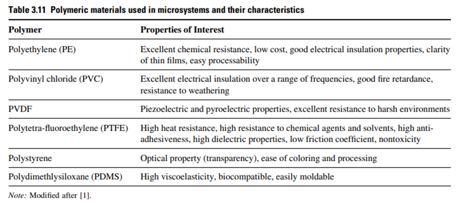
Some of the features which make polymers suitable for microscale applications are moldability, conformability, ease of deposition as thick and thin films. In addition, some polymers have conducting and semiconducting behaviors, while some others show pyroelectric effects in polymer side chains and these properties can be exploited. Properties of some of the commonly used polymers are listed in Table 3.11
Ceramic Materials
Ceramics are another major class of materials widely used in smart systems. These generally have good hardness and high-temperature strength. Thin and thick ceramic films and 3D ceramic structures are used in specialized microsystems applications; crystalline as well as noncrystalline materials are used.
For example, ceramic pressure microsensors have been developed for high-temperature environments, silicon carbide for harsh environments, etc. In addition to these structural ceramics, some functional ceramics, such as ZnO and PZT, have also been incorporated into smart systems.

