
Micro and Smart System Technology 4th Module
Semi-Conductor Diode
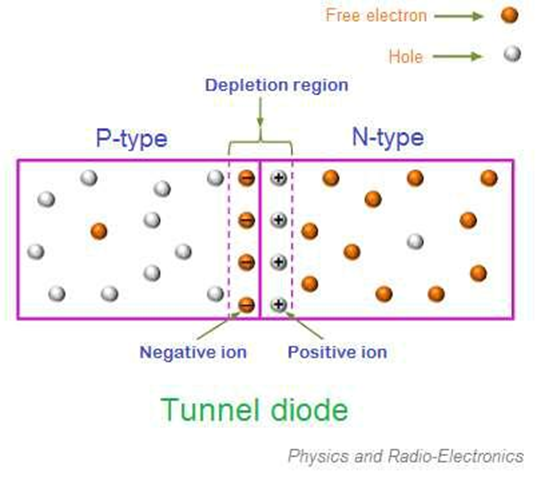
Discuss the working of Tunnel Diode.
Once no voltage is applied, then the n-type semiconductor material’s conduction band partly covers through the p-type material’s valence band. So this occurs due to heavy doping. The holes and electrons energy levels within the P-type & N-type remain the same correspondingly.
Once the temperature increases, electrons burrow from the n-region of the conduction band to the p-region of the valence band. In the same way, the holes burrow from the p-regions valance band to the n-region conduction band. So in this condition, the diode will be unbiased which means there is no flow of current through the diode.
Once the small voltage is applied to this diode, then zero electrons flow across the depletion region & zero current supplies throughout the diode. In the n-region, the few electrons from the conduction band are burrow into the valence band in the p-region due to the burrowing of electrons, so little forward current will supply throughout the depletion region.
Once the high voltage is applied to the tunnel diode, then charge carriers like holes & electrons will be generated. When the applied voltage increases then both the bands will overlap and the energy levels at both bands in two regions will be equal. Therefore, the highest current flows through the tunnel.
Once the applied voltage is again highly increased then both the bands of the diode are misaligned slightly. However, both the bands in the two regions still overlap. The little current supplies throughout the diode then the tunnel current will start reducing.
Applications of Tunnel Diode
- Tunnel diode can be used as a switch, amplifier, and oscillator.
- Since it shows a fast response, it is used as high frequency component.
- Tunnel diode acts as logic memory storage device.
- They are used in oscillator circuits, and in FM receivers. Since it is a low current device, it is not used more.
Define p-n juction diode & Explain working Principal of p-n junction diode. (semiconductor diode)
A p-n junction is an interface or a boundary between two semiconductor material types, namely the p-type and the n-type, inside a semiconductor.
Forward bias of PN junction diode
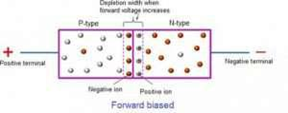
The diode is forward biased. The positive terminal of the battery is connected to the anode of a diode and negative terminal to the cathode.
Due to majority charge carriers the external applied voltage of forward bias is opposed by the barrier voltage and the diode does not conduct the current.
The applied voltage is increased above the barrier potential, it overcome the opposition of barrier potential and diode conducts the current due to majority carriers.This current is known as forward current and flows from anode to cathode through the diode.
Reverse bias of PN junction diode
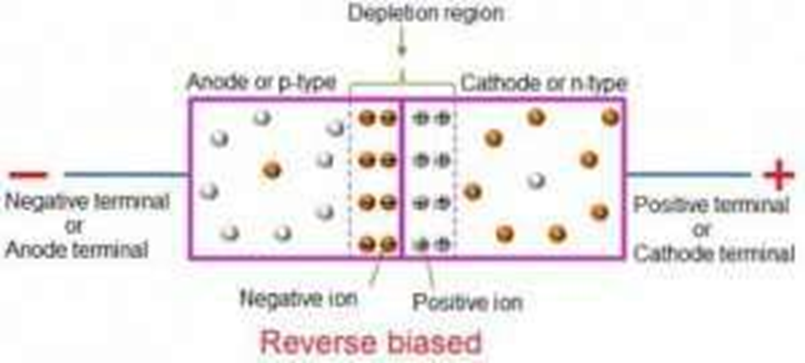
The negative terminal of the battery is connected to the anode of a diode and positive terminal of battery is connected to cathode. Hence, the diode is reverse bias.
When diode is reverse biased, majority carriers are blocked and only a small current flows through the diode due to the minority charge carriers.
As the reverse voltage is increased from zero, the reverse current very quickly reaches its saturation value which is also called as leakage current or reverses saturation current
Junction Diode Symbol and Static I-V Characteristics
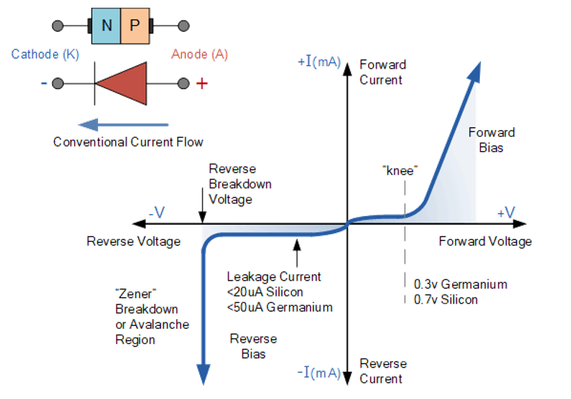
There are two operating regions and three possible “biasing” conditions for the standard Junction Diode and these are:
- 1. Zero Bias – No external voltage potential is applied to the PN junction diode.
- 2. Reverse Bias – The voltage potential is connected negative, (-ve) to the P-type material and positive, (+ve) to the N-type material across the diode which has the effect of Increasing the PN junction diode’s width.
- 3. Forward Bias – The voltage potential is connected positive, (+ve) to the P-type material and negative, (-ve) to the N-type material across the diode which has the effect of Decreasing the PN junction diodes width.
Diode Applications
Following are the applications and uses of the diode:
- Diodes as a rectifier
- Diodes in the clipping circuit
- Diodes in clamping circuits
- Diodes in logical gates
- Diodes in reverse current protection
With neat diagram explain the working of Schottky Diode.
Junction diode symbol and working-
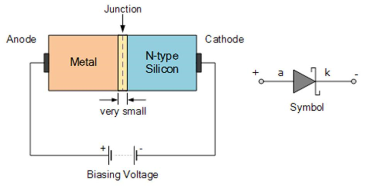
The operation relies on the principle that the electrons in different materials have different potential energy.
N-type semiconductors have higher potential energy than electrons of metals.
When these two are brought into contact, there is a flow of electrons in both directions across the metal-semiconductor interface.
A voltage is applied to the Schottky so that the metal is positive when compared to the semiconductor.
The voltage opposes the built-in potential and makes the current flow easy.
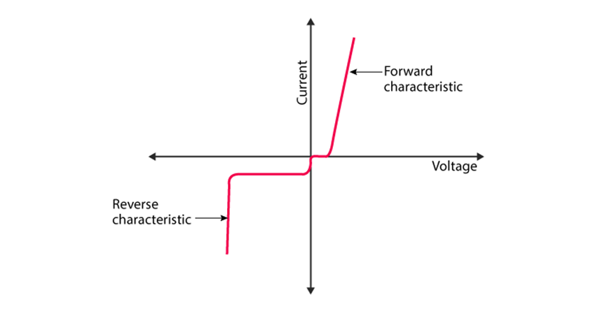
V-I Characteristics of Schottky Diode
The V-I characteristics of Schottky diodes are very much similar to the PN junction diode. Current is the dependent variable while voltage is the independent variable in the Schottky diode. The forward voltage drop of the Schottky diode is low between 0.2 to 0.3 volts.
Applications-
1. RF mixer and detector diode
2. Power rectifier
3. Power OR circuits
4. Solar Cell Applications
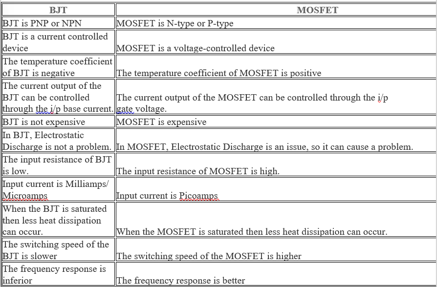
Bipolar Junction Transistor
A Bipolar Junction Transistor (also known as a BJT or BJT Transistor) is a three-terminal semiconductor device consisting of two p-n junctions which are able to amplify or magnify a signal. It is a current controlled device. The three terminals of the BJT are the base, the collector and the emitter. A BJT is a type of transistor that uses both electrons and holes as charge carriers.
here are two types of bipolar junction transistors – NPN transistors and PNP transistors. A diagram of these two types of bipolar junction transistors is given below.
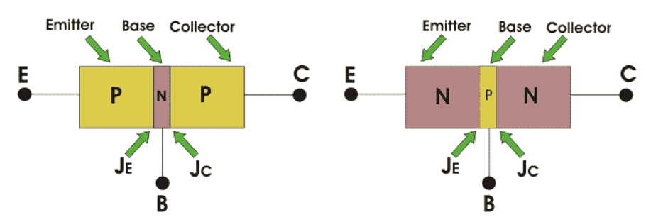
From the above figure, we can see that every BJT has three parts named emitter, base and collector. JE and JC represent the junction of emitter and junction of collector respectively. Now initially it is sufficient for us to know that emitter based junction is forward biased and collector-base junctions are reverse biased. The next topic will describe the two types of these transistors.
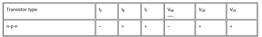
NPN Bipolar Junction Transistor
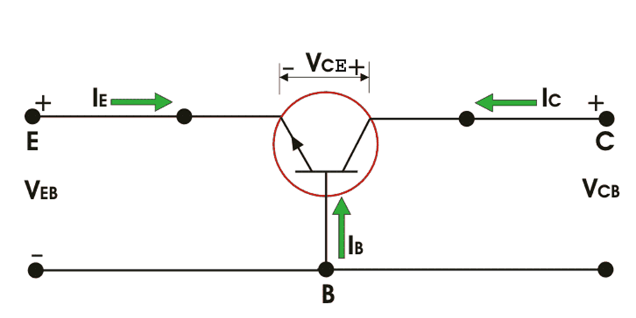
In an n-p-n bipolar transistor (or npn transistor) one p-type semiconductor resides between two n-type semiconductors the diagram below an n-p-n transistor is shown
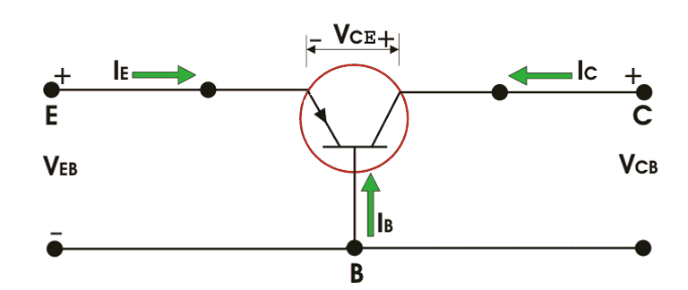
Now IE, IC is emitter current and collect current respectively and VEB and VCB are emitter-base voltage and collector-base voltage respectively. According to the convention if for the emitter, base and collector current IE, IB and IC current goes into the transistor the sign of the current is taken as positive and if current goes out from the transistor then the sign is taken as negative. We can tabulate the different currents and voltages inside the n-p-n transistor.
PNP Bipolar Junction Transistor
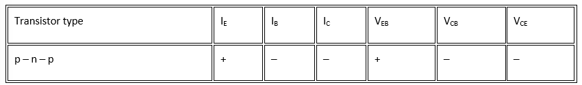
Similarly for p-n-p bipolar junction transistor (or pnp transistor), an n-type semiconductor is sandwiched between two p-type semiconductors. The diagram of a p-n-p transistor is shown below
For p-n-p transistors, current enters into the transistor through the emitter terminal. Like any bipolar junction transistor, the emitter-base junction is forward biased and the collector-base junction is reverse biased. We can tabulate the emitter, base and collector current, as well as the emitter-base, collector base and collector-emitter voltage for p-n-p transistors also.
Applications of BJT
We know that a bipolar junction transistor is used as a switch, as an amplifier, as a filter, and even as an oscillator. Below is the list of other applications of bipolar junction transistor:
- BJT is used as a detector or also known as a demodulator.
- BJT finds application in clipping circuits so that the waves can be shaped.
- Logic circuits and switching circuits use BJT.
MOSEFT
Enhancement mode:When positive voltage is applied to the gate terminal, it starts conducting and the current starts to flow
Depletion mode:The MOSFET is ON by default. When negative voltage is applied to the gate terminal it operates in the depletion mode and when positive voltage is applied, it operates in the enhancement mode.
Working of Enhancement MOSFET:
the enhancement mode the applied Gate voltage is always positive. When it crosses the threshold voltage it turns ON. The current is generated due to the movement of majority carriers. In N channel majority carriers are electrons and in P channel majority carriers are holes. The source is connected to the negative terminal. When the electrons move from source to drain the positive charges formed below the dielectric because of the repulsive force from gate combine with each other.
When the applied gate voltage is increased the number of majority carriers becomes more than the minority carriers below the dielectric medium. So the majority carriers overcomes the recombination of holes and electrons and the majority carrier move from source to drain in the channel, which forms the current. Thus the gate voltage controls the concentration of the majority carriers which is responsible for the formation of the channel
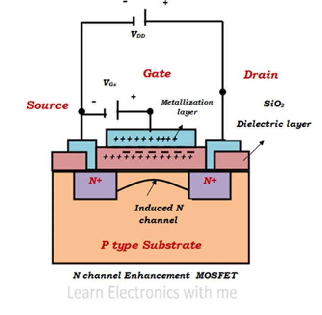
construction of n-channel MOSFET.
The metallic gate terminal in the MOSFET is insulated from the semiconductor layer by a SiO2 layer or dielectric layer. The MOSFET consists of three terminals, they are source(S), Gate (G), Drain (D) and the body which is called as substrate. The substrate is connected to the source internally.
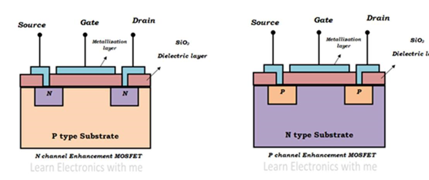
Construction of N channel and P channel Enhancement MOSFET
In N channel Enhancement MOSFET the source and drain are of N type semiconductor which is heavily doped and the Substrate is of P type semiconductor. Majority charge carriers are electrons. The source and drain terminals are physically separated in Enhancement mode.
In P channel Enhancement MOSFET the source and drain are of P type semiconductor which is heavily doped and the Substrate is of N type semiconductor. Majority charge carriers are hole
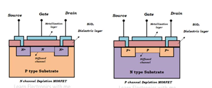
Construction of N channel and P channel Depletion MOSFET
In the N Channel depletion MOSFET a small strip of semiconductor of N type connects the source and drain. The source and drain are of N type semiconductor and the Substrate is of P type semiconductor. Majority charge carriers are electrons. The source and drain are heavily doped.
MOSFET applications
- Radiofrequency applications use MOSFET amplifiers extensively.
- MOSFET behaves as a passive circuit element.
- Power MOSFETs can be used to regulate DC motors.
- MOSFETs are used in the design of the chopper circuit.
CMOS Circuits
CMOS is a major class of ICs used in microprocessors, microcontrollers, and several other digital logic circuits.
CMOS Inverter
The inverter circuit as shown in the figure below. It consists of PMOS and NMOS FET. The input A serves as the gate voltage for both transistors.
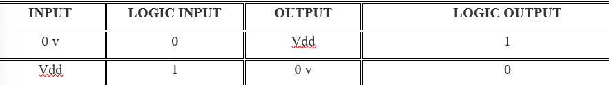
The NMOS transistor has input from Vss (ground) and the PMOS transistor has input from Vdd. The terminal Y is output. When a high voltage (~ Vdd) is given at input terminal (A) of the inverter, the PMOS becomes an open circuit, and NMOS switched OFF so the output will be pulled down to Vss.
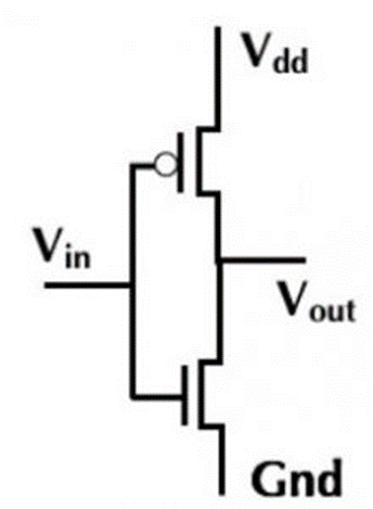
When a low-level voltage (<Vdd, ~0v) applied to the inverter, the NMOS switched OFF and PMOS switched ON. So the output becomes Vdd or the circuit is pulled up to Vdd.
CMOS NAND Gate
The below figure shows a 2-input Complementary MOS NAND gate. It consists of two series NMOS transistors between Y and Ground and two parallel PMOS transistors between Y and VDD.
If either input A or B is logic 0, at least one of the NMOS transistors will be OFF, breaking the path from Y to Ground. But at least one of the pMOS transistors will be ON, creating a path from Y to VDD.
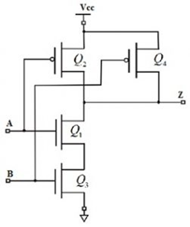
Two Input NAND Gate
Hence, the output Y will be high. If both inputs are high, both of the nMOS transistors will be ON and both of the pMOS transistors will be OFF. Hence, the output will be logic low. The truth table of the NAND logic gate given in the below table.
CMOS NOR Gate
A 2-input NOR gate is shown in the figure below. The NMOS transistors are in parallel to pull the output low when either input is high. The PMOS transistors are in series to pull the output high when both inputs are low, as given in the below table. The output is never left floating.
Two Input NOR Gate
|
A |
B |
Y |
|
0 |
0 |
1 |
|
0 |
1 |
0 |
|
1 |
0 |
0 |
|
1 |
1 |
0 |
The truth table of the NOR logic gate given in the below table.
CMOS Applications
Complementary MOS processes were widely implemented and have fundamentally replaced NMOS and bipolar processes for nearly all digital logic applications. CMOS technology has been used for the following digital IC designs.
· Computer memories, CPUs
· Microprocessor designs
· Flash memory chip designing
· Used to design application-specific integrated circuits (ASICs)
CMOS Characteristics
The most important characteristics of CMOS are low static power utilization, huge noise immunity. When the single transistor from the pair of MOSFET transistor is switched OFF then the series combination uses significant power throughout switching among the two stated like ON & OFF.
CMOS Working Principle
In CMOS technology, both N-type and P-type transistors are used to design logic functions. The same signal which turns ON a transistor of one type is used to turn OFF a transistor of the other type. This characteristic allows the design of logic devices using only simple switches, without the need for a pull-up resistor.
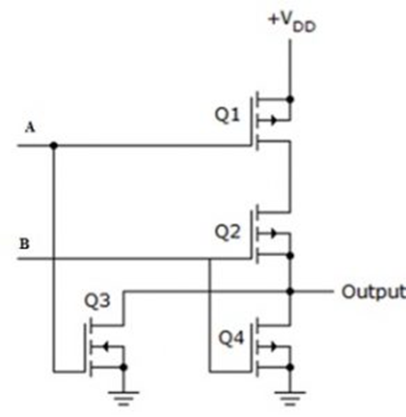
In CMOS logic gates a collection of n-type MOSFETs is arranged in a pull-down network between the output and the low voltage power supply rail (Vss or quite often ground). Instead of the load resistor of NMOS logic gates, CMOS logic gates have a collection of p-type MOSFETs in a pull-up network between the output and the higher-voltage rail (often named Vdd).
CMOS using Pull Up & Pull Down
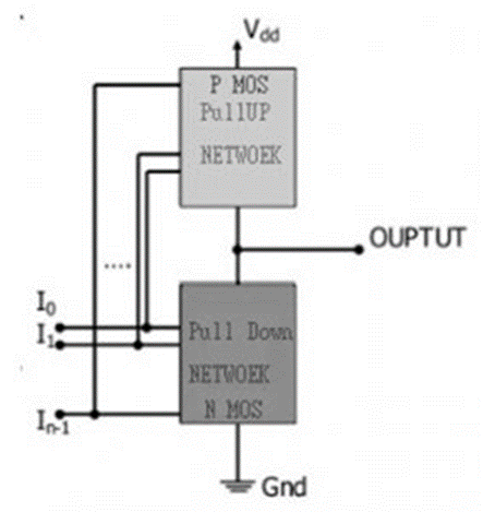
Thus, if both a p-type and n-type transistor have their gates connected to the same input, the p-type MOSFET will be ON when the n-type MOSFET is OFF, and vice-versa. The networks are arranged such that one is ON and the other OFF for any input pattern as shown in the figure
Op-Amp based circuits
1. Voltage Follower
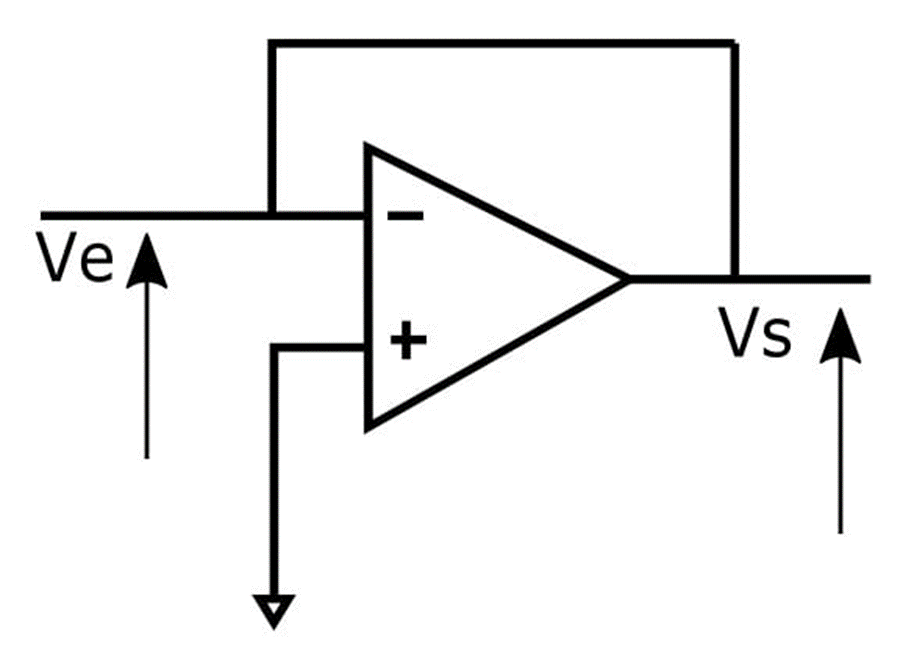
The most basic circuit is the voltage buffer, as it does not require any external components.
This circuit allows for the creation of a very high impedance input and low impedance output. This is useful to interface logic levels between two components or when a power supply is based on a voltage divider.
Applications -Buffer stage to prevent loading of a circuit by the next stage.
2. Inverting Op Amp
In this configuration, the output is fed back to the negative or inverting input through a resistor (R2). The input signal is applied to this inverting pin through a resistor (R1).
The positive pin is connected to ground.
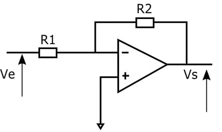
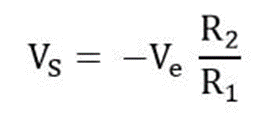
This is evident in the special case where R1 and R2 are equal. This configuration allows for the production of a signal that is complementary to the input, as the output is exactly the opposite of the input signal.
Due to the negative sign, the output and input signals are out of phase. If both signals must be in phase, a non-inverting amplifier is used.
Application: At the applications where the signal must be balanced inverting amplifiers are utilized.
3. Non-inverting Op Amp
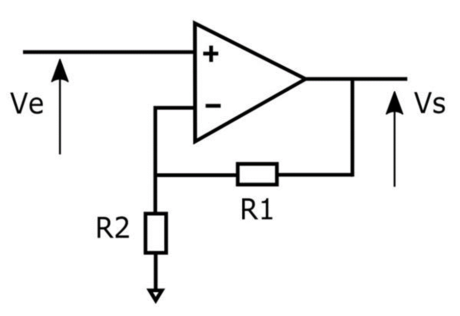
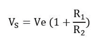
This configuration is very similar to the inverting operation amplifier. For the non-inverting one, the input voltage is directly to the applied to the non-inverting pin and the end of feedback loop is connected to ground.
These configurations allow amplification of one signal. It’s possible to amplify several signals by using summing amplifiers.
Application: Weinbridge oscillator circuits (to realize the amplifier of gain= 3)
4. Non-inverting Summing Amplifier
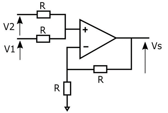
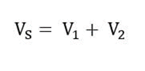
To add 2 voltages, only 2 resistors can be added on the positive pin to the non-inverting operational amplifier circuit.
It is worth noticing that adding several voltages is not a very flexible solution. Indeed, if a 3rd voltage is added with exactly the same resistances, the formula would be Vs = 2/3 (V1 + V2 + V3).
The resistors would need to be changed to get Vs = V1 + V2 + V3, or a 2nd option is to use an inverting summer amplifier.
Application - Audio Mixer
5. Inverting Summing Amplifier
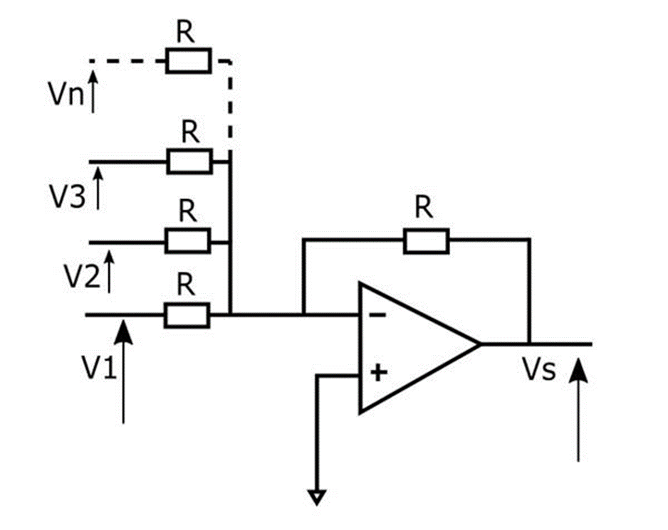
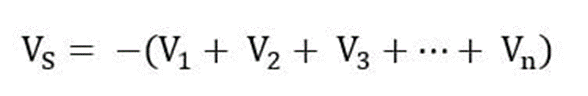
By adding resistors in parallel on the inverting input pin of the inverting operation amplifier circuit, all the voltages are summed.
Unlike the non-inverting summing amplifier, any number of voltages can be added without changing resistor values.
Application: Digital to Analog Converter (DAC)
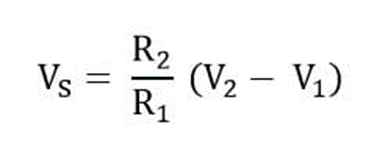
6. Differential Amplifier
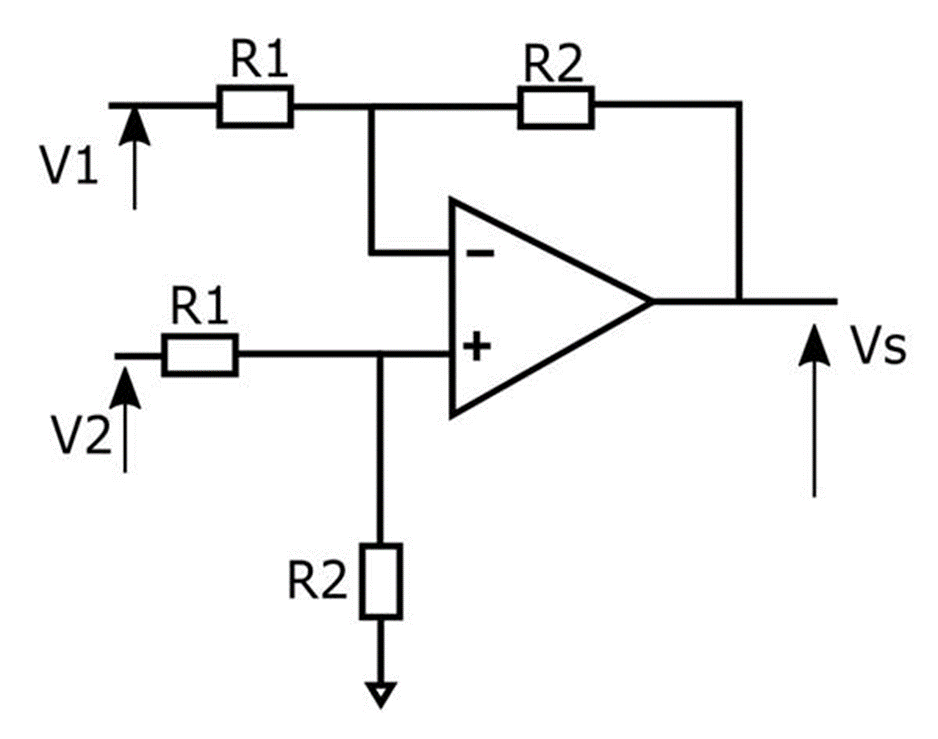
The inverting operational amplifier (see circuit number 2) amplified a voltage that was applied on the inverting pin, and the output voltage was out of phase. The non-inverting pin is connected to ground with this configuration.
If the above circuit is modified by applying a voltage through a voltage divider on the non-inverting, we end up with a differential amplifier as shown below.
An amplifier is useful not just because it lets you add, subtract, or compare voltages. Many circuits allow you to modify signals. Let’s see the most basic ones.
Applications:
The differential operational amplifier can be used as an automatic gain control circuit.
7. Integrator
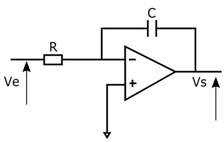
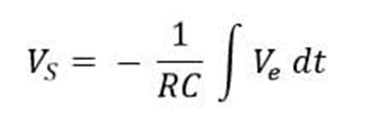
A square wave is very easy to generate, by just toggling a GPIO of a microcontroller for example. If a circuit needs a triangle waveform, a good way to do it is just integrating the square wave signal. With an Operation Amplifier, a capacitor on the inverting feedback path, and a resistor on the input inverting pin as shown below, the input signal is integrated.
Be aware that a resistor is often connected in parallel to the capacitor for saturation issues. Indeed, if the input signal is a very low frequency sine wave, the capacitor acts like an open circuit and blocks feedback voltage. The amplifier is then like a normal open-loop amplifier that has very high open-loop gain, and the amplifier is saturated. Thanks to a resistor in parallel of the capacitor, the circuit behaves like an inverting amplifier with a low frequency, and saturation is avoided.
Application - To generate sawtooth voltage from a square wave input
8. Op Amp Differentiator
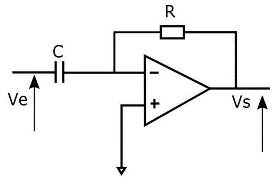
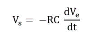
The differentiator works similarly to the integrator by swapping the capacitor and the resistor.
All the configurations that were presented up to now.
Applications- To generate a square wave voltage from a sawtooth input voltage.

