Sensors and Signal Conditioning 5th Module
INTRODUCTON
Sensors based on semiconductor junctions are of twofold interest. First, the large yield of microfabrication processes results in very competitive prices for them. Second, it is possible to include sensor, signal conditioning, signal processing, and communication circuits to produce intelligent sensors.
The journal Sensors and Actuators reports on scientific research in sensors (and actuators) based on semiconductors (in general). The magazine Sensorscovers industrial developments.
5.1 THERMOMETRES BASED ON SEMICONDUCTOR JUNCTIONS
The forward characteristic for a diode is temperature-dependent (about -2 mV/C for silicon diodes),which is usually considered a shortcoming. However, we can use that dependence to measure temperature or any other quantity related to a change in temperature.
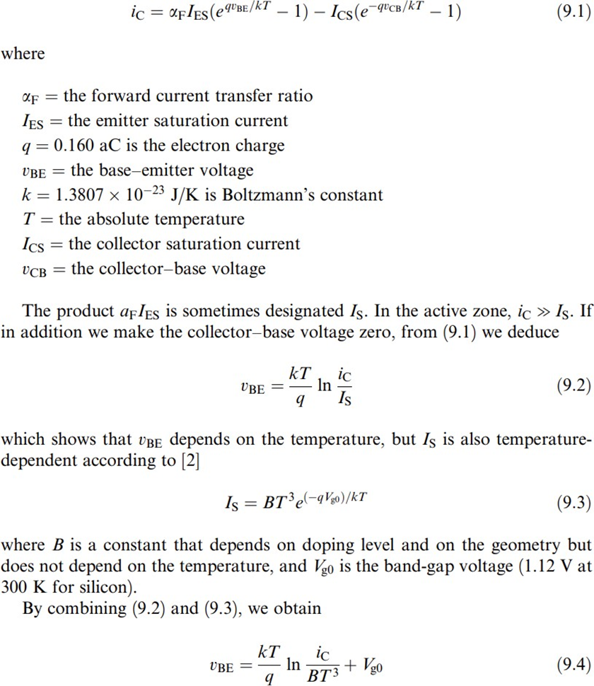
But this dependence is nonlinear and not repetitive enough for accurate measurements. It is therefore better to use the temperature dependence of the base-emitter voltage vBE of a transistor supplied with a constant collector current.
According to the Ebers Moll model, the collector currentfor an ideal transistor is
5.2 MAGNETO DIODES AND MAGNETO TRANSISTORS
I±V characteristics for a diode change in a magnetic field perpendicular to the direction of travel of charge carriers because the Lorentz force deviates those carriers from their trajectories. If a diodeis designed so that the carriers are deviated to a high recombination region, then the I±V characteristic of the resulting magneto diode depends on the magnetic field intensity. The sensitivity to the magneticfield increases when recombination characteristics for the high and low recombination regionsdiffer substantially. This sensitivity is about ten times higher than that of a silicon Hall-effect device. However, magnetodiodes need unconventional IC processes that are expensive.
This same principle can be appliedto magneto transistor design, but anotherstructure is preferred, which consists of a base, an emitter,and two collector.
An alternative sensor uses a Hall element and two transistors. The Hall element is the base common to both transistors and has two contacts, one at each base. When a magneticfield generates a Hall voltagebetween both contacts, the base voltage for one transistor is larger than that for the other,thus resulting in collector current imbalance, which is a measure of the appliedfield. It is also possibleto arrange the Hall elementso that it controls the gate voltage of a field-effect transistor.
None of these devices has yet found broad commercial use, mostly becauseof their poor repeatability, low sensitivity, and offset problems.
5.3 PHOTO DIODES AND PHOTO TRANSISTORS
The internal photoelectric effect in a p-n junction results in a change in the contact potentialor in the short-circuit current,which depends on the intensity of the incident radiation. Photodiodes are based on the same principle; but instead of using them as self-generating sensors, we apply an inverse bias voltage, usually from 5 V to 30 V. This increases the width of the depletionregion and yields a faster response time and a current proportional to the radiationintensity.
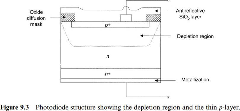
Figure 9.3 shows the structure for a photodiode. Because nondepleted p and n regions are conductive, any applied voltage is applied to the depletion region, where it creates an electric field. Any incident radiation absorbed produces electron-hole pairs, which accumulate in the p and n regions because of the electric field, thus resulting in a voltage (photovoltaic effect). In order to collect the output current, charges have to migrate to the diode surface, which slows the response time. This results in a higher recombination probability, which reduces the responsivity (sensitivity).
A phototransistor is an integrated combination of photodiode and n-p-n transistor where the optical radiation illuminates the base. The collector current i

where ip and iD and b is the current gain for the transistor in the common emitter configuration (from 100 to 1000). This gain is not constant but depends on the current and therefore on the illumination level. This lack of linearity and also their lower bandwidth as compared to photodiodes (due to the large base-collector capacitance) makes them less suitable for measurement.
Phototransistors, however, suit switching applications because of their current gain. For applications requiring gains up to 100,000, photo- Darlingtons are available that consist of a phototransistor feeding the base of a second transistor. Phototransistors work in the wavelength range from 0.4 mm to 1.1 mm.
Phototransistors are extensively used in photoelectric sensing for industrial applications.
Photoelectric sensing uses a light source (LED for color applications) and a photoelectric sensor and phototransistor that responds to a change in the intensity of the light falling upon it. Applications requiring high sensitivity to visible light use photoconductors. Applications requiring a very fast response or a linear response over a broad range of irradiance use photodiodes. The emitted light is modulatedby turning the LED on and off at severalkilohertz. The amplifierfollowing the phototransistor is tuned to the modulation frequency so that interfering light signals that is, those not pulsing at the same frequency are rejected.
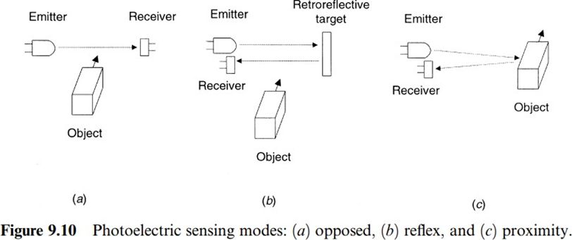
There are three basic photoelectric sensing modes:opposed, retro reflective, and proximity. In the opposed sensing mode, also referred to as through- beam, beam-break, or direct scanning, the light from the emitter is directly aimed at the receiver.
In the retroreflective sensing mode, also termed reflex,or retro for short, the emitter aims the light beam at the retroreflective target, which bounces it back to the receiver (Figure 9.10b). An object is sensed when it interrupts the beam,provided that it is not highly reflective.
In proximity mode sensing the object establishes a light beam rather than interrupts it. The emitterand the receiverare on the same side of the object.
The emitter sends energy and the receiverdetects the energyreflected from the object (Figure 9.10c).Bright white surfacesare sensed at a greaterrange than dull black surfaces. Also, large objects return more energy than small objects.Lens systems focus the emittedlight to an exact point in front of the sensor, and they also focus the receiver at thesame point.
5.4 SENSORS BASED ON MOSFET TRANSISTORS
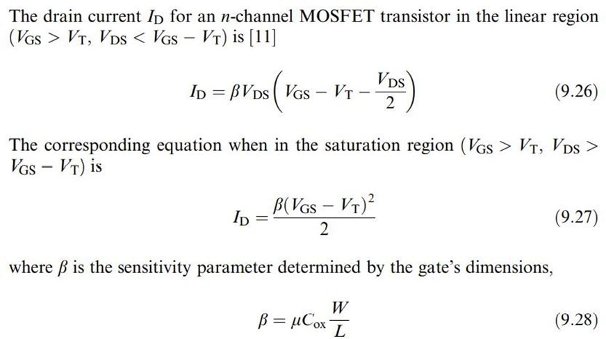
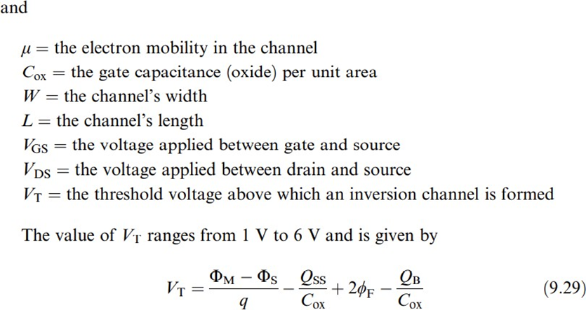
When MOSFET transistors are used as electronic components, we assume that all parameters in equations (9.26 ) through (9.29) are constant. By so doing, we obtain a well-defined input-output relationship between VG and ID.
In sensors, on the contrary, we are interested in detecting quantities that modulate some of these parameters . However, this fact is common to many electronic devices, and MOSFET transistors are not frequently used for those applications. The important advantage for MOSFET transistors is the dependence between VT and the work function (or chemical potential) for the metal, FM [12].FETs sensitive to chemicals are termed ChemFETs.
The simplest modification is just to omit the gate. The best-known one consists of interposing a given material between gate and oxide, thus rendering the transistor sensitive to any measurand resulting in changes in that material.
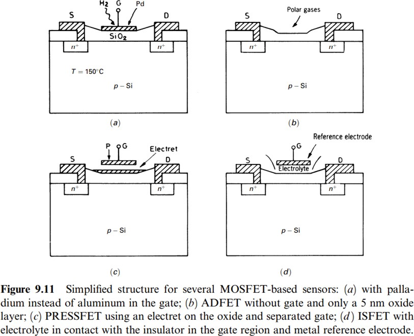
An ISFET (ion-sensitive FET ) is a MOSFET transistor that instead of gate electrode has in that region a chemically selective covering or membrane. When it is immersedinto an electrolyte, the potential in the insulation (oxide)
depends on the detected ion concentration. That potential depends on the threshold voltage and therefore on the drain current. The reference metal electrode immersedin the same electrolyte can be considered as the equivalent to the gate electrode (whichis not present in the device).
5.5 CHARGE COUPLED SENSORS
A CCD is a monolithic array of closelyspaced MOS capacitors that transfers an analog signalcharge (a “packet'') from one capacitorto the next, working as an analog shift register. The charge is stored and transferred between potential wells at or near an Si-SiO2 interface (Figure 9.12). These wells are formed by MOS capacitors (an array of metal electrodes is deposited on the SiO2) pulsed by a multiphase clock voltage. The charges transferred are electrons or holes, respectively, in n-channel and p-channel devicesand can be introduced either electrically or optically. For optical input the CCD acts as optical sensor.
If in Figure 9.12 a positive step voltage is applied to a gate electrode while adjacent electrodes remain at a lower voltage, a potential-energy well is set up into the p substrate, and charge (electrons) is stored underthat electrode. If now one of the adjacent electrodes is biased with a voltage higher than that of the previous electrode, a deeper potential well is established and the stored charge travels to it along the surface of the silicon to seek the lowest potential. By clocking electrode voltages, we can thus move, in a given direction, the charge initiallystored. However, thermalelectron-hole pairs are being continuously produced, and electronseventually fill the well. Therefore, a CCD is a dynamicdevice in which we can store a charge signalonly for a time much shorter than thermal relaxation times for the MOS capacitors.
In the so-called buried channel CCD, which is the commonest, instead of storing and transferring the charge at the silicon surface under the silicon dioxide, those processes happen in a buried channelaway from the Si-SiO2 interface. This yields an increased carriermobility, hence speed, and independence of surface phenomena (whichresult in noise and losses).
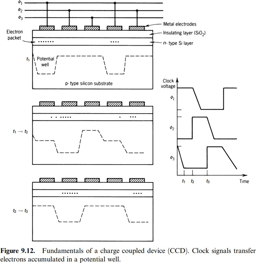
In a CCD image sensor, light from the object illuminates a CCD, either from the electrode or from the substrate side, and electron-hole pairs are created in the silicon by the photoelectric effect. (Silicon is sensitive to photons withwavelengths from 300 nm to 1100 nm.) By applying the appropriate clock signals,potential wells are created that collect the photon-generated minoritycarriers for a time called the optical integration time, while majority carriers are swept into the substrate. The collected chargepackets are shifteddown the CCD register and converted into voltage or current at the outputterminal. The amount of charge accumulated in each well is a linear function of the illumination intensity and the exposure (or integration) time. The output signal charge is a stepped dc voltage that will linearly vary from a thermally generated background level (noise) at zero illumination (dark condition) to a maximum at saturation under bright illumination.
TYPES OF CCD IMAGE SENSORS
There are two types of CCD imagersavailable: the line imager and the areaimager. The number ofpixels ranges from 128 to 16 million.Common linear models have from 1800 to 5400 pixels. Typical pixel sizes are 27 mm2 for 512 - 512 arrays and 12 mm2 for 1024 - 1024 arrays. Line imagers (Figure 9.15) have a line of sensor elements, also called photo-sites or pixels, with a common electrode called a photogate and an individual optical microlens.
Pixels are electrically separated from one another by a highly concentrated p-type region called a channel stop. Some model shave some additional msensing elements shielded from external light by an opaque metallization (aluminum) that provide a dark reference level.
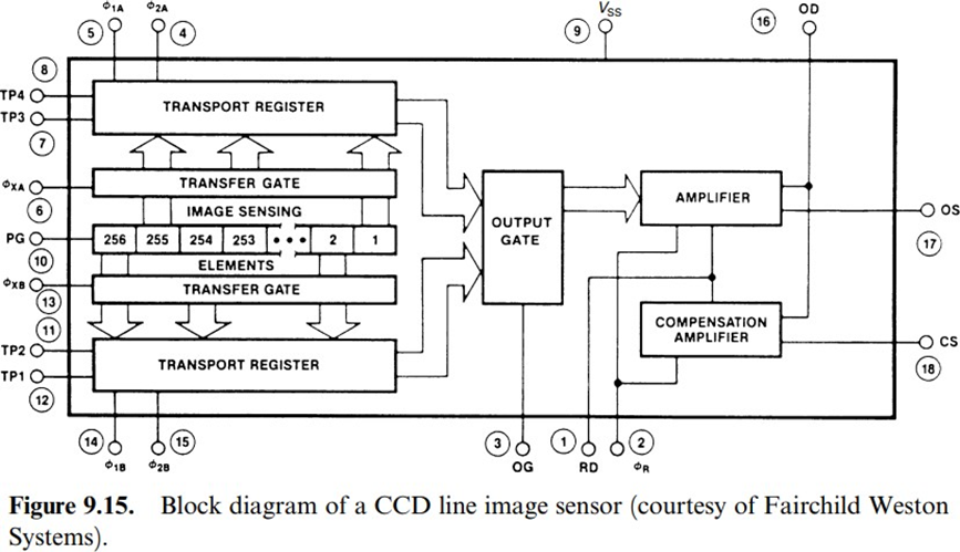
Adjacent to the line of sensor elements, there is a structure called a charge transfer gate, arranged in two lines, one at each side of the row of sensors. When the transfer gate voltage goes high and the photogate goes low, the photon-generated charge packets, which have accumulated at each pixel when the photogate voltage was high, are alternately transferred into the transfergate storage well, with odd-numbered pixels to one side, even to the other side. From the transfer gates the charge packets are transferred to the transport registers and moved serially to the output amplifier. The transfer gate also controls the integration time. Transfer gatesprevent image smear,which is a fundamental limitation of the basic CCD image sensor; it is due to the pickup of spurious charge by charge packets while they are transferred and lightis still incident on the array.
The main parameters of line image sensors are spatial resolution, responsivity, spectral response, dynamic range, and output data rate. The spatial resolution characterizes the ability to discriminate between closely spaced points in the image. It is expressed by the modulation transfer function (MTF ) of the output, which depends on the spatial frequency of an image..The intensity modulation of an image with a given spatial frequencyfocused on the image sensor yields a modulation depth of the output, which decreases at high spatial frequencies. The MTF is the output modulationdepth normalized to unity at zero spatialfrequency
APPLICATIONS, ADVANTAGES AND DISADVANTAGES
CCD imaging sensorsare used in solid-state TV cameras and other imagingdevices working with visibleor infrared light,where an opticalsystem focuses the image on the sensor. The precise knowledge of photosensor locations with respectto one another gives them a definiteadvantage as comparedto vacuum tube TV cameras.
It’s low-power and low-voltage requirements make them even more attractive, particularly for hand-held devices such as camcorders. They are used, for example, in inspection, measurement, surveillance, telecine, facsimile, spectrometers, and optical character recognition (high-speed mail sorting, currencysorting, document scanning,etc.), in activities ranging from food processing to astronomy (spacetelescopes), and in technological fieldsranging from roboticsto cartography and medical imaging.
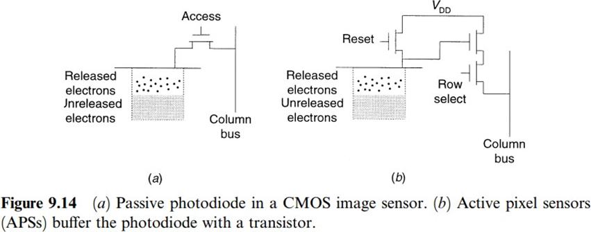
CCDs have superior dynamic range, lower FPN, and higher sensitivity to light than CMOS image sensors. However, CMOS sensors need ten times less power than CCDs and their support chips, work with a single power supply, integrate support circuitry in the same chip as the sensor, and allow random pixel access,
5.6 ULTRASONIC BASED SENSORS
Ultrasound is a mechanical radiation with a frequency above the human hearing range (about 20 kHz). As for any radiation, when ultrasound strikesobject, part is reflected, part is transmitted, and part is absorbed. In addition, when the radiation source moves relative to the reflector, there is a shift in received frequency (Doppler effect). The penetration power for ultrasound permitsnoninvasive applications; that is, thereis no need to installhardware where the changes to be detectedoccur. Noninvasive measurements are of interestin explosive and radioactive environments, in medical applications
and also to prevent contamination of the medium where measurements are performed. Noninvasive sensors are generally easier to install and maintainthan invasive sensors.
ULTRASONIC BASEDSENSING METHODS AND APPLICATIONS
Ultrasonic-based sensors are usually based on their transit time,attenuation, or velocity. Most of them use piezoelectric ceramics or polymer transducers as generators and detectors. They must work at a temperature below the respective Curie point. The resolution is limited by the wavelength, which is inversely proportional to the frequency

But high frequencies have larger attenuation than low frequencies. Spurious vibrations from industrial noise may interfere with the receiver.Using systems with narrow sound beams reduces interference from background noise. Maximal power is radiated axially (i.e., perpendicularly) to the transducer face, so the sensitivity and range depend on the relative position between transducer and reflector.
Transit time ultrasonic sensors emit an ultrasonic burst and measure the elapsed time between transmission and reception (echo ranging). The elapsed time multiplied by the speed of sound equals twice the distance to the impedance discontinuity that returns the echo. Smooth,non porous surfaces reflect sound better than rough or porous surfaces.
Poor reflectors return stronger echoes at low frequencies [20]. Non-flat surfaces return low-level echos. The minimal distance between transducerand reflector depends on the time required for the transducer to extinguish echoes (ringing)resulting from the transmitted burst. Ringing lasts longer for lower frequencies. Evaluating a series of pulses rather than a single pulse reduces interference from background noise. Because air turbulence may blow off echoes, ultrasonic sensors are not suitable for outdoor use.
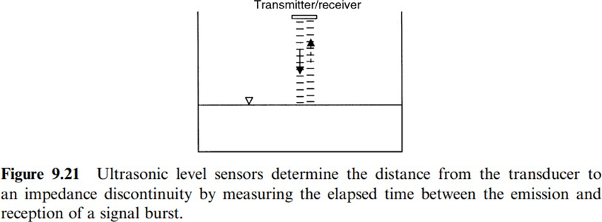
For liquid or solid levelmeasurement, the transducer is usually placedabove the tank and transmits a cone-shaped beam pattern (Figure 9.21). Theacoustic impedance of air and liquids or solids (including powders) is so different that most of the energy propagating in one of them is reflected when reaching the interface.
Dielectric constant, conductivity, color, viscosity, and specific gravity do not affect accuracy, but vapors, fumes, and dust do. Placingthe sensor inside a stilling well reduces effectsof surface agitation in liquids.
Foamy or fluffy surfaces absorb energy, hence reducing effectiveness. The sensor can alternatively be placed at the bottomof the tank so that the soundpropagates in the liquid or solid, but then the transducer and cabling must be leakproof.
Object detection and proximity switches can rely on the disruption of the sound beam as the object passes between the transmitter and the receiver, similar to beam-through photoelectric sensing (Figure 9.10a).Sensors based on ultrasonic attenuation have been applied to air or foam bubble detectors in plastic, glass, or metal tubing for example, to prevent air embolism in patients.Some of the most widely used sensorsbased on ultrasonic velocity are ultrasonic Doppler flowmeters. Any substance having acoustic impedancedifferent from that of the flowing fluidcan act as reflector and shift the fre-
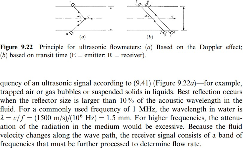
Ultrasonic flowmeters neither produce any pressure loss, nor contaminate the fluid. They cause no wear and can measure hot and cold fluids and slurries. They are routinely used in industry to measure liquids, gases, and two-phase or multiphase fluids. They are the method of choice to estimate arterial blood flow rate noninvasively. The dependence of sound velocity on temperature has been applied to measure the temperature of water in oceans and gases in chimneys.


