Analog and Digital Electronics 2nd Module
MODULE 2: OSCILLATORS AND COMPARATORS
Oscillator Principles
An oscillator is a type of feedback amplifier. In which part of the output is feedback to the input via a feedback circuit. If the signal feedback is of proper magnitude and phase, the circuit products alternating currents or voltages. To visualise the requirements of an oscillator, consider the block diagram of fig. 7
However, here the input voltage is zero (Vin = 0). Also, the feedback is positive because most oscillators use positive feedback. Finally, the closed loop gain of the amplifier is denoted by Av rather than AF.
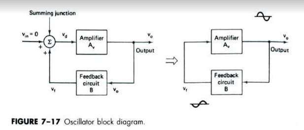
In the block diagram of figure 7
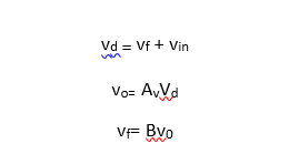
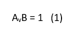
Using these relationships, the following equation is obtained:

However, vin = 0 and v0≠ implies that
Expressed in polar form,
Equation 2 gives the two requirements for oscillation
AvB = 1/0° or 360° (2)
1. The magnitude of the loop gain AvB must be atleast 1
2. The total phase shift of the loop gain AvB must be equal to 0° or 360°
For instance in figure 7, if the amplifier causes a phase shift of 180°, the feedback circuit must provide an additional phase shift of 180°, so that phase shift around the loop is 360°.
The Waveforms shown in fig 7 are sinusoidal and are used to illustrate the circuit’s action. The type of waveform generated by an oscillator depends on the component and hence may be sinusoidal, square or triangular.
The frequency of the oscillation is determined by the components in the feedback circuit.
Oscillator Types
|
Types of components used |
Frequency of Oscillation |
Types of waveform generated |
|
RC oscillator |
Audio frequency |
Sinusoidal |
|
LC oscillator |
Radio Frequency |
Square Wave |
|
Crystal Oscillators |
|
Triangular Wave Sawtooth wave etc |
Frequency Stability
The ability of the oscillator circuit to oscillate at one exact frequency is called frequency stability. Although a number of factors may cause changes in oscillator frequency, the primary factors are temperature changes and changes in the dc power supply.
Temperature and power supply changes cause variations in the op=amp’s gain, in junction capacitances and resistances of the transistors in an op-amp,and in external circuit components. In most cases these variations can be kept small by careful design, by using regulated power supplies, and by temperature control.
Another important factor that determines frequency stability is the figure of merit Q of the circuit. The higher the Q, the greater the stability. For this reason, crystal oscillators are far more stable than RC or LC oscillators, especially at higher frequencies.
Phase Shift Oscillator
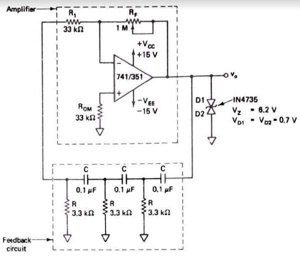
Fig 7.18 shows a phase shift oscillator, which consists of an op-amp as the amplifying stage and three RC cascaded networks as the feedback circuit. The feedback circuit provides feedback voltage from the output back to the input of the amplifier.
The op-amp is used in the inverting mode; therefore, any signal that appears at the inverting terminal is shifted by 180° at the output. An additional 180° phase shift required for oscillation is provided by the cascaded RC networks. Thus, the total phase shift around the loop is 360°.
At some specific frequency when the phase shift of the cascaded RC networks is exactly 180° and the gain of the amplifier is sufficiently large, the circuit will oscillate at that frequency.
This frequency is called frequency of oscillation, f0 and is given by

At this frequency, the gain Av must be at least 29. That is,

Thus the circuit will produce a sinusoidal waveform of frequency fo if the gain is 29 and the circuit will produce a sinusoidal waveform of frequency fo if the gain is 29 and the total phase shift around the circuit is exactly 360°. For a desired frequency of oscillation, choose a capacitor C, and then calculate the value of R from equation 2.
A desired current amplitude, however can be obtained with back to back zeners connected at the output terminal
Design the phase shift oscillator of fig 7.18 so that fo = 200Hz (Important)
Or
Design and explain the working of RC phase shift oscillator for fo = 200Hz
(solve the problem first and then explain phase shift oscillatorand then draw diagram )
Let C = 0.1 µ𝐹. Then, from the equation

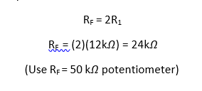
To prevent the loading of the amplifier because of RC networks, it is necessary that R1≥ 10R. Therefore let R1=10R = 33𝑘𝛺. Then from RF = 29R1
RF = 29(33 k𝛺) = 957k𝛺 (Use RF = 1-M𝛺 potentiometer)
When choosing an op-amp, type 741 can be used at lower frequencies (<1kHz)
Wien Bridge Oscillator
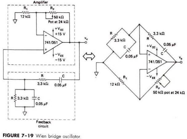
Because of its simplicity and stability, one of the most commonly used audio frequency oscillators is the Wien Bridge. Fig shows the Wien Bridge oscillator in which the Wien bridge circuit is connected between the amplifier input terminals and the output terminal. The bridge has a series RC network in one arm and a parallel RC network in the adjoining arm. In the remaining two arms of the bridge, resistors R1 and RF are connected
The phase angle criterion for oscillation is that the total phase shift around the circuit must be 0°. This condition occurs only when the bride is balanced, that is, at resonance. The frequency of oscillation f0 is exactly the resonant frequency of the balanced Wien bridge and is given by

Assuming that the resistors are equal in value, and the capacitors are equal in value in the reactive leg of the Wien bridge. At this frequency the gain required for sustained oscillation is given by

Design the Wien bridge oscillator of fig 7.19 so that fo =965Hz
(same procedure as phase shift)
Let C = 0.05µ𝐹. therefore from equation

Now, let R1 = 12 k𝛺. Then from equation
Comparator
A comparator is an electronic circuit, which compares the two inputs that are applied to it and producesan output. The output value of the comparator indicateswhich of the inputs is greater or lesser.
Basic Comparator
Inverting Comparator
An inverting comparator is an op-amp based comparator for which a reference voltage is applied to its non-inverting terminal and the input voltage is applied to its inverting terminal. This comparator is called as inverting comparator because the input voltage, which has to be compared is applied to the inverting terminal of op- amp.

The circuit diagram of an inverting comparator is shown in the following figure.
The operation of an inverting comparator is very simple. It produces one of the two values, +Vsat and −Vsat at the output based on the values of its input voltage Vi and the reference voltage Vref.
· The output value of an inverting comparator will be −Vsat, for which the input Vi voltage is greater than the reference voltage Vref.
· The output value of an inverting comparator will be +Vsat, for which the input Vi is less than the reference voltage Vref.
The following figure shows the input and output waveforms of an inverting comparator, when the reference voltage is zero volts.
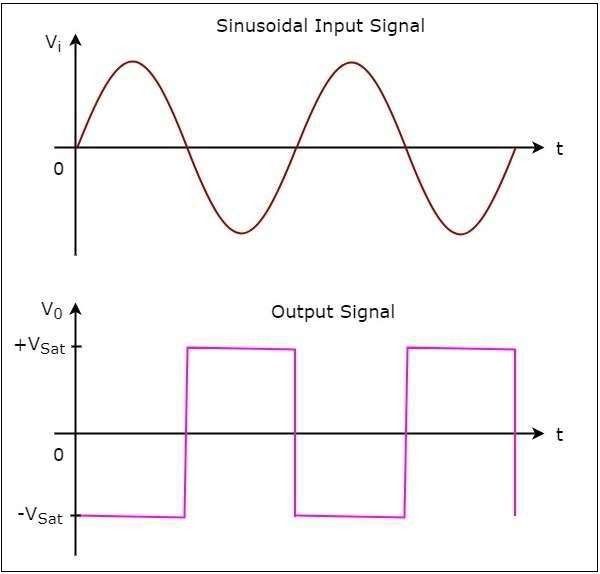
· In the figure shown above, we can observe that the output transitions either
from −Vsat to +Vsat or from +Vsat to −Vsat whenever the sinusoidal input signal is crossing zero volts. In other words, output changes its value when the inputis crossing zero volts. Hence, the above circuit is also called as inverting zero crossing detector.
Non-Inverting Comparator
A non-inverting comparator is an op-amp based comparator for which a reference voltage is applied to its inverting terminal and the input voltage is applied to its non- inverting terminal. This op-amp based comparator is called as non- inverting comparator because the input voltage, which has to be compared is applied to the non-inverting terminal of the op-amp.
The circuit diagram of a non-inverting comparator is shown in the following figure

The operation of a non-inverting comparator is very simple. It produces one of the two values, +Vsat and −Vsat at the output based on the values of input voltage Vt and the reference voltage +Vref.
· The output value of a non-inverting comparator will be +Vsat for which the input voltage Vi is greater than the reference voltage +Vref.
· The output value of a non-inverting comparator will bee −Vsat, for which the input voltage Vi is less than the reference voltage +Vref.
The following figure shows the input and output waveforms of a non-inverting comparator, when the reference voltage is zero volts.
· From the figure shown above, we can observe that the output transitions eitherfrom +Vsat to −Vsat or from −Vsat to +Vsat whenever the sinusoidal input signal crosses zero volts. That means, the output changes its value when the input is crossing zero volts. Hence, the above circuit is also called as non-inverting zero crossing detector.
Zero Crossing Detector
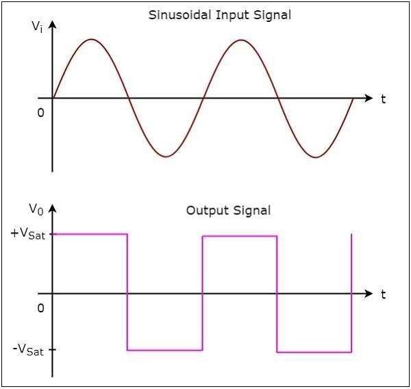
An immediate application of the comparator is the zero-crossing detector or sine wave-to- square wave converter. The basic comparator can be used as the zero crossing detector provided that Vref is set to zero.
Fig a shows the inverting comparator used as a zero-crossing detector. The output voltage v0waveform in fig b shows when and in what direction an input signal vin crosses zero volts. That is, the output v0 is driven into negative saturation when the input signal vin passes through zero in the positive direction, Conversely, when vin passes through zero in the negative direction, the output vo switches and saturates positively.
Schmitt Trigger
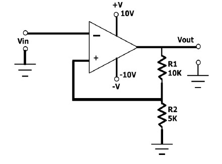
Fig 8.4 (a) shows an inverting comparator with positive feedback. This circuit converts an irregular shaped waveform to a square wave or pulse. The circuit is known as the Schmitt trigger or squaring circuit.
Upper Threshold Voltage
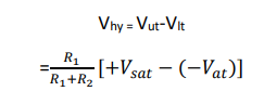
The input voltage vin triggers the output vo every time in exceeds certain voltage level called the upper threshold voltage Vut and lower threshold voltages that depends on the value and polarity of the output voltage v0.
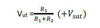
When vo= +Vsat, the voltage across R1 is called the upper threshold voltage, Vut. The input voltage vin must be slightly more positive than Vut in order to cause the output voto switch from + Vsat to -Vsat, As long as vin < Vut, vois at + Vsat. Using the voltage-divider rule,
Lower Threshold Voltage
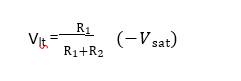
On the other hand, when vo= -Vsat, the voltage across R1, is referred to as the lower threshold voltage, Vlt. Vin must be slightly more negative than Vit in order to cause voto switch from -V sat to +V sat. In other words for vin values greater than Vlt, vois at -Vsat. Vit is given by the following equation
Hysteresis Characteristics
The comparator with positive feedback is said to exhibit hysteresis, a dead-band condition. That is when the input of the comparator exceeds Vut, its output switches from +Vsat to -Vsat and reverts back to its original state, +Vsat, when the input goes below Vlt (see figure 8.4c). The hysteresis voltage is, of course, equal to the difference between Vut and Vlt. Therefore