
Micro and Smart System Technology 2nd Module
A sensor is a device that receives and responds to a signal. This signal must be produced by some type of energy, such as heat, light, motion, or chemical reaction. Once a sensor detects one or more of these signals (an input), it converts it into an analog or digital representation of the input signal.
Basic Example of sensor is the human body, Eyes detect light energy, ears detect acoustic energy, a tongue and a nose detect certain chemicals, and skin detects pressures and temperatures. The eyes, ears, tongue, nose, and skin receive these signals then send messages to the brain which outputs a response.
A transducer is any device which converts one form of energy into another.
Examples of common transducers include the following:
A microphone converts sound into electrical impulses and a loudspeaker converts electrical impulses into sound (i.e., sound energy to electrical energy and vice versa).
A solar cell converts light into electricity and a thermocouple converts thermal energy into electrical energy.
An actuator is a device that actuates or moves something. An actuator uses energy to provide motion. Therefore, an actuator is a specific type of a transducer.
Examples-
An incandescent light bulb produces light by passing a current through a filament. Thus, a light bulb is a transducer for converting electrical energy into optical energy.
An electric motor is a transducer for conversion of electricity into mechanical energy or motion
The desirable features of sensors are:
1. Range / span
2. Errors and accuracy
3. Non-linearity
4. Hysteresis
5. Dead band and Saturation
6. Output impedance
7. Repeatability
8. Reliability
9. Sensitvity
10.Resolution
11.Frequency Response
12.Response time
Difference between Sensor and Actuator :
|
SENSOR |
ACTUATOR |
|
It converts physical characteristics into electrical
signals. |
It converts electrical signals into physical
characteristics. |
|
It takes input from environment. |
It takes input from output conditioning unit of system. |
|
It gives output to input conditioning unit of system. |
It gives output to environment. |
|
Sensor generated electrical signals. |
Actuator generates heat or motion. |
|
It is placed at input port of the system. |
It is placed at output port of the system. |
|
It is used to measure the physical quantity. |
It is used to measure the continuous and discrete process
parameters. |
|
It gives information to the system about environment. |
It accepts command to perform a function. |
|
Example: Photo-voltaic cell which converts light energy
into electrical energy. |
Example: Stepper motor where electrical energy drives the
motor. |
|
|
|
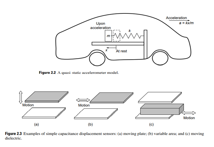
Silicon Capacitive accelorometer
An accelerometer can be thought of as a mass suspended by a spring. When there is acceleration, there will be a force on the mass. The mass moves, and this movement is determined by the spring constant of the suspension. By measuring the displacement, we can get an estimate of the acceleration (Figure 2.2).
A capacitor may be formed with two plates of which one is fixed while the other moves [Figures 2.3(a), (b)]. In another arrangement, the mass can move in between two plates [Figure 2.3(c)]. In all three, the capacitance changes according to the motion caused by acceleration
Advantages of Silicon Capacitive Accelerometers
Silicon capacitive accelerometers have:
1. Very low sensitivity to temperature-induced drift.
2. Higher output levels than other types.
3. Amenability for force-balancing and hence for closed-loop operation.
4. High linearity.
Typical Applications
Typical applications of silicon capacitive accelerometers include:
1. Consumer: airbag deployment systems in cars, active suspensions, adaptive brakes, alarm systems, shipping recorders, home appliances, mobile phone, toys, etc.
2. Industrial: crash-testing robotics, machine control, vibration monitoring, etc.
3. High-end applications: military/space/aircraft industry navigation and inertial guidance, impact detection, tilt measurement, high-shock environments, cardiac pacemaker, etc
Piezoresistive pressure sensor
Figure 2.6 shows the cross-section and top view of a pressure sensor die. When the diaphragm deforms due to the pressure to be measured, the resistances of the piezoresistors change. Calculation of piezoresistive responses in real structures must take account of the fact that piezoresistors are typically formed by diffusion and hence have nonuniform doping. They also span a finite area on the device and hence have nonuniform stress.
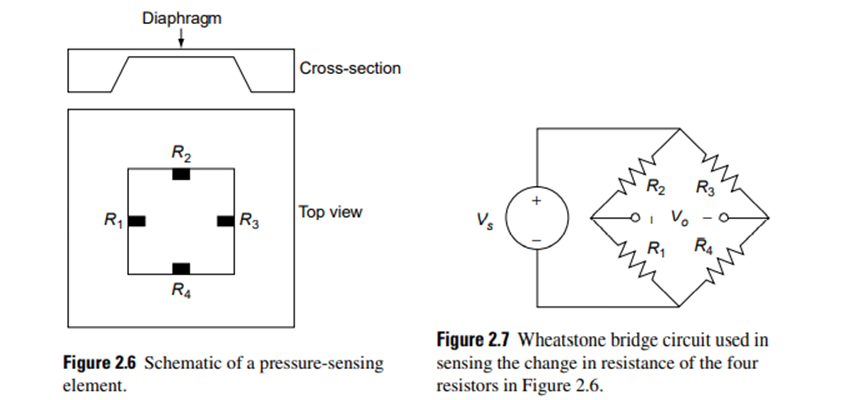
For complete representation of all effects, one should solve the Poisson equation for the electrostatic potential throughout the piezoresistor, subject to boundary conditions of applied potentials at its contacts and subject to stress induced by deformation of the structural elements. From this potential, one determines the electric field, then the current density, and finally the total current.
However, because the direction of current flow is along the resistor axis and, except at the contacts, parallel to the surface, considerable simplification is possible. Furthermore, the change in resistance due to stress is small, typically 2% or less. The Wheatstone bridge used to measure the change in resistance is shown in Figure 2.7
Advantages of Piezoresistive Pressure Sensors
Micromachined piezoresistive pressure sensors have:
1. Compact size, making them suitable for a variety of applications, including those that use an array of such sensors to measure pressure distribution.
2. Good thermal stability, since thermal compensation can be built into the sensor.
3. Good market potential due to low cost.
Typical Applications
Typical applications of piezoresistive pressure sensors include:
1. Direct pressure-sensing applications: such as weather instrumentation, combustion pressure in an engine cylinder or a gasturbine, appliances such as washing machines, etc.
2. Altitude-sensing applications: such as in aircraft, rockets, satellites, weather balloons, where the measured pressure is converted using an appropriate formula.
3. Flow-sensing applications, manifold pressure sensing: in automobiles, etc
CONDUCTOMETRIC GAS SENSOR
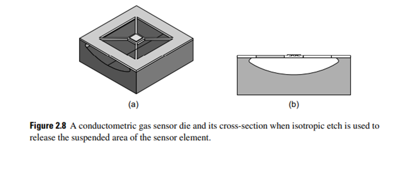
An active area suspended by four beams off the fixed part of the wafer is the main element of this gas sensor in Figure 2.8. The adsorption or reaction of a gas on this active surface of the semiconducting material induces a change in the density of the conducting electrons in the polycrystalline sensor element. This change in conductivity is detected using electronic circuitry.
The chemical reaction can be described in four steps:
1. Preadsorption of oxygen on semiconducting material surface.
2. Adsorption of a specific gas.
3. Reaction between oxygen and adsorbed gas.
4. Desorption of reacted gas on the surface.
The above process of delivering electrons between the gas and the semiconductor actually represents the sensitivity of the gas sensor. While reacting with the gas, the conductivity of the semiconductor gas sensor decreases when the adsorbed oxygen molecules play the role of the acceptor, whereas the conductivity increases when the adsorbed oxygen molecules play the role of the donor.
The principle is based upon initial reversible reaction of atmospheric oxygen with lattice vacancies in the oxide and the concurrent reduction in electron concentration. This reaction generates various oxygen species according to the temperature and oxygen pressures, that is, O2, O-, O2 -, which can then react irreversibly with certain combustible species.
Metal electrodes deposited on the top of the formed membrane that contains the active area make the measurement of the resistance of the gas-sensitive layer possible. Generally, the electrodes are located underneath the sensing film. Usually, the electrode materials are gold and platinum and, in some cases, aluminum or tungsten.
Application(s) Environmental monitoring, automotive application, air conditioning in airplanes, spacecraft, living spaces, sensor networks, breath analyzers, food control applications, etc
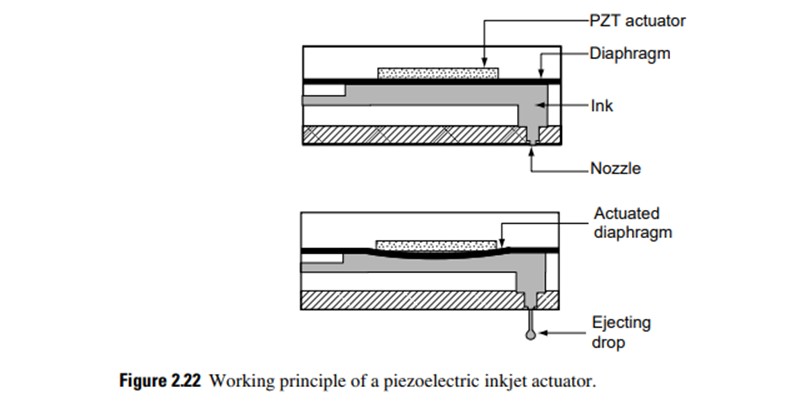
Piezoelectric Inkjet Printer
Piezoelectric effect: a behavior of special materials in which an electrical field causes mechanical strain and vice versa.
A print head for a piezoelectric inkjet printer includes a piezoelectric actuator in the form of a plate, which lies on one side of a plate. The actuator includes drive electrodes. The plate has pressure chambers each aligned with one of the drive electrodes. The cavity plate also has nozzles, each communicating with one of the chambers.
When a voltage is applied, the PZT disk attached to the diaphragm experiences a strain and deforms, as shown in Figure 2.22. When the deformation of the diaphragm begins, the ink in the chamber is pressurized and starts to move through the nozzle. When the diaphragm deflects further, the ink drop separates and is ejected, as shown in Figure 2.22.
Application(s) Paper printing, biochip production, etc
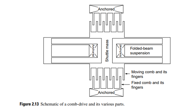
.Electrostatic Comb-drive
A top-view schematic of a comb-drive is shown in Figure 2.13. It consists of a shuttle mass suspended by a planar folded-beam suspension. The shuttle mass has combs attached to it. These moving combs interleave with the combs that are anchored to the substrate. When an electric voltage is applied, the moving comb fingers try to align with the fixed comb fingers. By alternating the voltage on the top and bottom fixed combs while keeping the moving combs at ground voltage, the shuttle mass can be made to move to and fro.
The same arrangement can be used for measuring capacitance. A pair of moving and fixed fingers forms a parallel-plate capacitor. By packing a number of such pairs, we can get sufficiently large capacitance. The capacitance change is larger when the moving comb moves along the gap between itself and the fixed finger rather than along the length. So, when used as a sensor, the folded-beam suspension is turned by 90
Application(s) Actuators: resonators, microgrippers, force balancing accelerometers and microscanners. Sensors: automotive, aerospace, machine tools, biomedical, space applications, etc
Magnetic MicroRelay
A Relay is an electromechanical device that can be used to make or break an electrical connection.
Types of Relay Based on the principle of operation
• Electrothermal relay:
When two different materials are joined together it forms into a bimetallic strip. When this strip is energized it tends to bend, this property is used in such a way that the bending nature makes a connection with the contacts.
• Electromechanical relay:
With the help of few mechanical parts and based on the property of an electromagnet a connection is made with the contacts.
• Solid State relay:
Instead of using mechanical parts as in electrothermal and electromechanical relays, it uses semiconductor devices. So, the switching speed of the device can be made easier and faster. The main advantages of this relay are its more life span and faster switching operation compared to other relays.
• Hybrid relay:
It is the combination of both electromechanical and solid-state relays.
A schematic of a magnetic microrelay is shown in Figure 2.15. The magnetic flux is generated when a current passes through the excited coil. Most of the flux is concentrated in the permalloy magnetic core. The permalloy cantilever, represented as a spring in the schematic, is attracted by the magnetic force and then bends down to connect to the fixed contact.
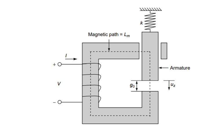
The active armature is also a conductor; hence, the current will flow from the active armature to the fixed contact when the active armature connects to the fixed contact, and then the relay will stay in the ON state. The active armature is forced to leave the fixed contact by the spring’s restoring force when the exciting current is cut off, and then the relay stays in the OFF state.
Applications Automotive, computer, medical, etc.
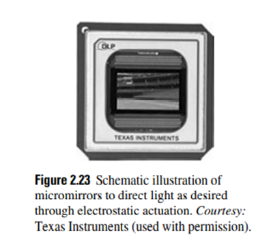
Micromirror Array for Video Projection
The data for the image to be projected is fed to the chip that is integrated with the micromirror chip. The processor generates the actuation sequence of the mirrors for the particular image. This sequence is fed one by one in to the S-RAM cell beneath the mirror corresponding to each frame. The cell changes the bias voltage of the electrodes, which results in an electrostatic torque.
This torque works against the restoring torque of the hinges to produce mirror-and-yoke rotation in the positive or negative direction. The mirror and yoke rotate until the yoke comes to rest against mechanical stops at the same potential as the yoke. Because geometry, not a balance of electrostatic torques, determines the rotation angle, the rotation angle is precisely determined.
Now, the light is fed from a source such as an LED or a halide lamp. It is reflected from the mirror at an angle that depends up on the tilt of the mirror. In the ON position, the mirror reflects the light and lets it pass through the optical window on the chip cover. So the light emerges out of the chip.
In the OFF position, the mirror redirects the light to a heat sink inside the chip that absorbs the light and the heat. Now, by controlling the mirrors, different gray scales can be produced depending upon the relative timings of the ON and OFF positions. Thus, they can be used to recreate the image on the screen.
The materials used are:
1. Aluminum for mirrors.
2. Gold for better mirror-reflectivity.
3. Complementary metal-oxide-semiconductor (CMOS) substrate for electrodes.
4. Silicon dioxide for sacrificial layer.
5. Silicon nitride for electrical insulation.
Application(s) Commercial display devices especially DLPTM Projectors, HDTV, optical routers in high speed fiber optic communication network
Portable blood analyser
This blood analyzer needs a small blood sample (0.3 ml). The blood enters the sensing region aided by a smart passive microfluidic manipulation system that includes a microdispensor, a unit multiplexer, and air-busting detonators. Here, application-specific biosensors such as oxygen sensors and glucose sensors perform analysis on a chip. Then, the information is sent to the application-specific integrated circuit (ASIC) and the results are displayed using a liquid crystal display (LCD). All this happens in a small hand-held device.
See for details. Contrast the above with what happens today. Depending upon the tests that have been ordered, a large quantity of blood sample is processed before it is analyzed. Most routine laboratory tests are performed on either plasma or serum. Plasma, the liquid portion of blood, is separated from the cellular portion of blood by rapidly spinning the specimen in a centrifuge for several minutes. Then the tests are performed on it. It takes several hours to get the result. Portable clinical analyzers of this type are made by Abbott Laboratories, Abbott Park, IL, U.S.A, [8]. Figure 2.18, a schematic of a lab-on-a-chip, shows how a stack of patterned polymer layers gives a platform for flowing fluids to perform biochemical reactions for sensing and analysing
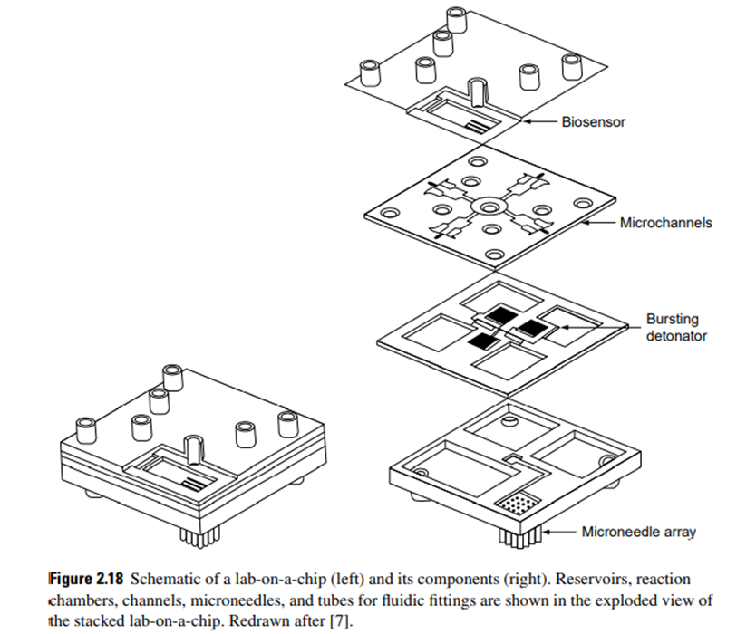
At the start of the operation sequence, the blood sample is loaded using microneedles. Then, the microdispenser reservoir is filled with the sample. When the air-bursting detonators break open, the liquid sample travels through the multiplexed channels. The divided sample reaches the biosensing reservoir on which the biosensors are mounted. When the sample is loaded into the sensor reservoir, the measurement cycle is initiated and the concentrations of the desired analytes are measured. The transduced signals are processed in the electronics.
Advantages of Portable Blood Analyzer
The following are the advantages of a portable blood analyzer:
1. Quick analysis of up to 50 blood parameters within a few seconds.
2. Provisions for recording and transmitting the results automatically.
Materials Used
The materials used for making portable blood analyzer are:
1. Cyclic olefin copolymer (COC): used for the substrate; this material is preferred over other polymers.
2. Silicon: used for the semipermeable membrane of the oxygen sensor because of its high permeability and low signal-to-noise ratio.
3. Polyurethane: used for the semipermeable membrane of the glucose/lactate sensor.
Fabrication Process
A fabrication process that combines polymer-processing techniques is needed here. Unlike silicon micromachining, these are not yet standardized. Typical processing techniques are: the replaceable mold disk technique, plasma treatment with reactive ion etching, thermoplastic fusion-bonding, spin-coating, and screen-printing.
Key Definitions
Important terms used and their definitions are:
1. sPROMs: a passive microfluidic control technique in which a set of microfluidic manipulations is carried out in a preprogramed sequence. The microfluidic operations and their sequence are determined primarily by the structural arrangement of the system without the need for an external control signal.
2. Microdispenser: a dispenser giving out graduated amounts of blood at a given time.
3. Multiplexer: a channel network carrying the required amount of sample from the common source point.
4. Air-bursting detonators: As the name suggests, compressed air bursts out from an encapsulated membrane in order to develop a pressure difference across the microfluidic network

